OP17 查看數據表(PDF) - Analog Devices
零件编号
产品描述 (功能)
生产厂家
OP17 Datasheet PDF : 12 Pages
| |||
TEST CIRCUITS
V+
100k⍀
2
7
5
1
6
3
4
NOTE:VOS CAN BE TRIMMED WITH POTENTIOMETERS
RANGING FROM 10k⍀ TO 1M⍀. FOR MOST UNITS
TCVOS WILL BE MINIMIZED WHEN VOS IS ADJUSTED
WITH A 100k⍀ POTENTIOMETER
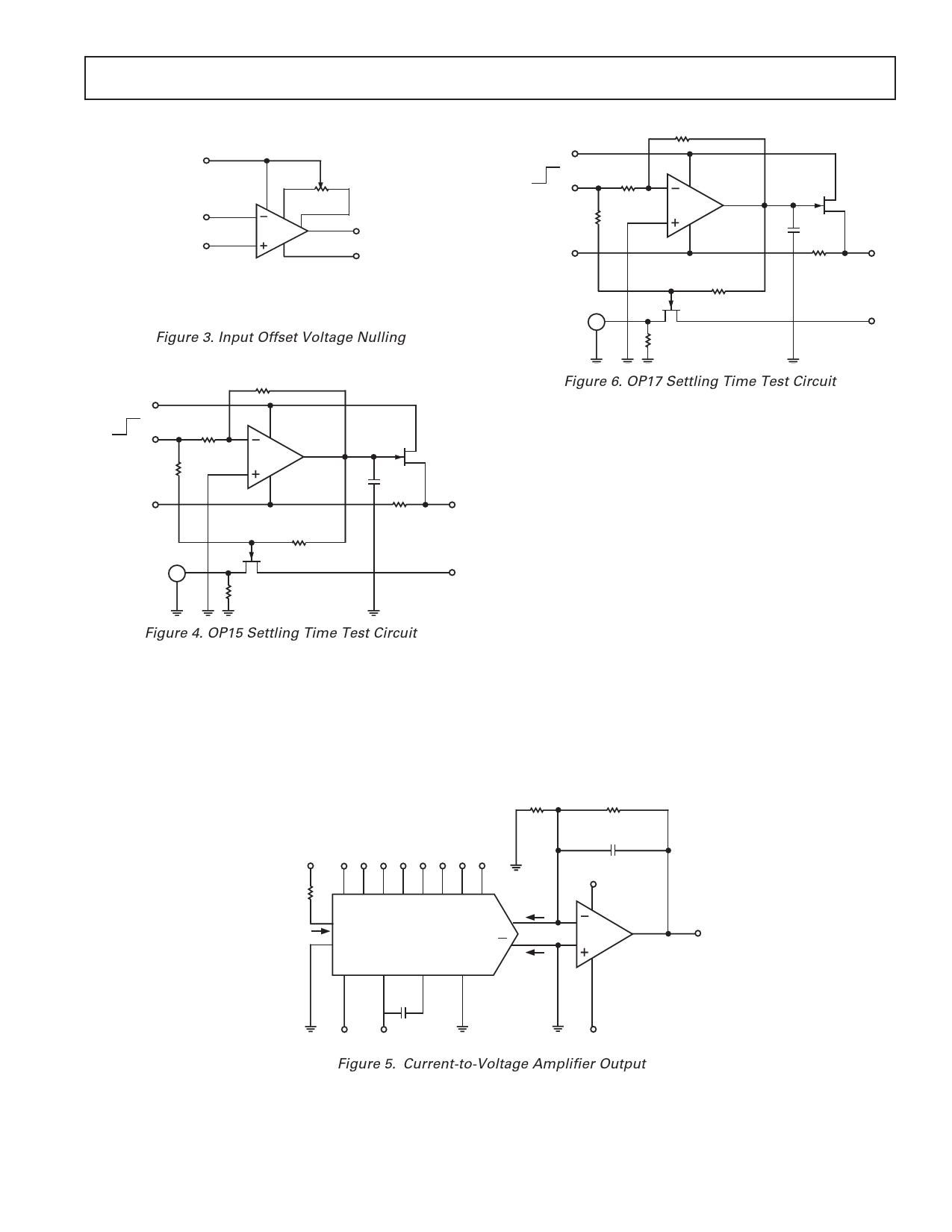
Figure 3. Input Offset Voltage Nulling
10V
0V
+15V
2k⍀
0.1%
5k⍀
0.1%
–15V
2k⍀
0.1% 2
7
OP15 6
3
4
SUMMING
NODE
5k⍀
0.1%
SCOPE
2N4416
2k⍀
2N4416
100pF
3k⍀
VOUT
AV = –1
+15V
Figure 4. OP15 Settling Time Test Circuit
OP15/OP17
10V
0V
+15V
2k⍀
0.1%
1k⍀
0.1%
–15V
400⍀
0.1% 2
7
OP17 6
3
4
SUMMING
NODE
5k⍀
0.1%
SCOPE
2N4416
2k⍀
2N4416
100pF
3k⍀
VOUT
AV = –1
+15V
Figure 6. OP17 Settling Time Test Circuit
APPLICATION INFORMATION
Dynamic Operating Considerations
As with most amplifiers, care should be taken with lead dress,
component placement and supply decoupling in order to ensure
stability. For example, resistors from the output to an input should
be placed with the body close to the input to minimize “pick-up”
and maximize the frequency of the feedback pole by minimizing
the capacitance for the input to ground.
A feedback pole is created when the feedback around any amplifier
is resistive. The parallel resistance and capacitance from the input
of the device (usually the inverting input) to ac ground set the
frequency of this pole. In many instances the frequency of this
pole is much greater than the expected, 3 dB frequency of the
close-loop gain, and consequently there is negligible effect on
stability margin. However, if the feedback pole is less than approxi-
mately six times the expected 3 dB frequency, a lead capacitor
should be placed from the output to the negative input of the op
amp. The value of the added capacitor should be such that the
RC time-constant of this capacitor and the resistance it parallels
is greater than, or equal to, the original feedback pole time is constant.
R1
R2
10k⍀
5k⍀
DIGITAL INPUTS
+10V MSB
LSB
RREF
5k⍀
5 6 7 8 9 10 11 12
B1 B2 B3 B4 B5 B6 B7 B8
14
VREF+
VREF–
15
DAC08E
V+
V–
CC
VLC
4
IO
IO
2
3
13 C1 16 1
0.1F
C2
30pF
+15V
7
2
6
OP15F
3
VO = 0V TO 10V
4
+15V –15V
–15V
Figure 5. Current-to-Voltage Amplifier Output
REV. A
–11–
Share Link: 