IDT74FCT16952AT 查看數據表(PDF) - Integrated Device Technology
零件编号
产品描述 (功能)
生产厂家
IDT74FCT16952AT Datasheet PDF : 7 Pages
| |||
IDT74FCT16925AT/CT/ET
FAST CMOS 16-BIT REGISTERED TRANSCEIVER
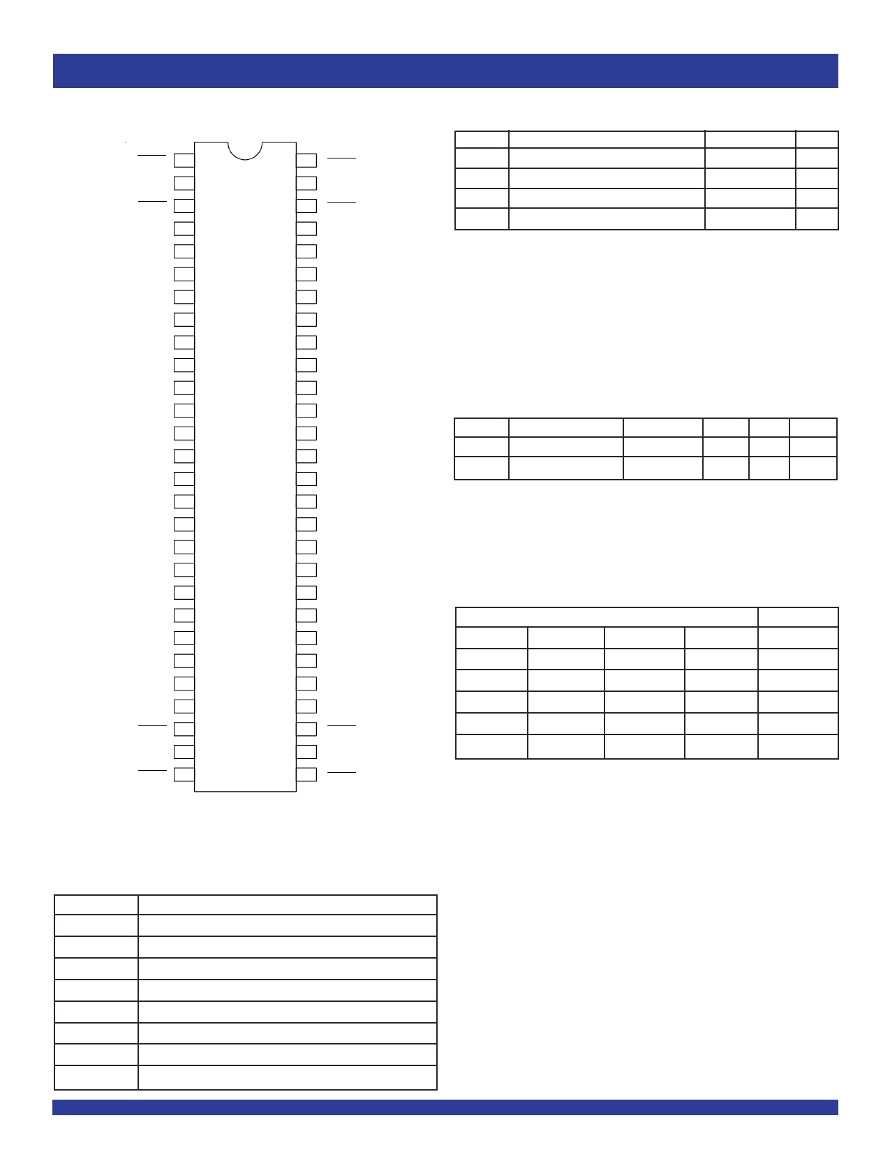
PIN CONFIGURATION
1OEAB
1CLKAB
1CEAB
GND
1A1
1A2
VCC
1A3
1A4
1A5
GND
1A6
1A7
1A8
2A1
2A2
2A3
GND
2A4
2A5
2A6
VCC
2A7
2A8
GND
2CEAB
2CLKAB
2OEAB
1
56
2
55
3
54
4
53
5
52
6
51
7
50
8
49
9
48
10
47
11
46
12
45
13
44
14
43
15
42
16
41
17
40
18
39
19
38
20
37
21
36
22
35
23
34
24
33
25
32
26
31
27
30
28
29
SSOP/ TSSOP
TOP VIEW
1OEBA
1CLKBA
1CEBA
GND
1B1
1B2
VCC
1B3
1B4
1B5
GND
1B6
1B7
1B8
2B1
2B2
2B3
GND
2B4
2B5
2B6
VCC
2B7
2B8
GND
2CEBA
2CLKBA
2OEBA
PIN DESCRIPTION
Pin Names
Description
xOEAB
A-to-B Output Enable Input (Active LOW)
xOEBA
B-to-A Output Enable Input (Active LOW)
xCEAB
A-to-B Clock Enable Input (Active LOW)
xCEBA
B-to-A Clock Enable Input (Active LOW)
xCLKAB
A-to-B Clock Input
xCLKBA
B-to-A Clock Input
xAx
A-to-B Data Inputs or B-to-A 3-State Outputs
xBx
B-to-A Data Inputs or A-to-B 3-State Outputs
INDUSTRIAL TEMPERATURE RANGE
ABSOLUTE MAXIMUM RATINGS(1)
Symbol
Description
Max
Unit
VTERM(2) Terminal Voltage with Respect to GND
–0.5 to +7
V
VTERM(3) Terminal Voltage with Respect to GND –0.5 to VCC+0.5 V
TSTG Storage Temperature
–65 to +150
°C
IOUT
DC Output Current
–60 to +120
mA
NOTES:
1. Stresses greater than those listed under ABSOLUTE MAXIMUM RATINGS may cause
permanent damage to the device. This is a stress rating only and functional operation
of the device at these or any other conditions above those indicated in the operational
sections of this specification is not implied. Exposure to absolute maximum rating
conditions for extended periods may affect reliability.
2. All device terminals except FCT162XXX Output and I/O terminals.
3. Output and I/O terminals for FCT162XXX.
CAPACITANCE (TA = +25°C, F = 1.0MHz)
Symbol
Parameter(1)
Conditions Typ. Max. Unit
CIN
Input Capacitance
VIN = 0V
3.5
6
pF
COUT
Output Capacitance VOUT = 0V
3.5
8
pF
NOTE:
1. This parameter is measured at characterization but not tested.
FUNCTION TABLE(1,3)
Inputs
xCEAB
xCLKAB
xOEAB
H
X
L
X
L
L
L
↑
L
L
↑
L
X
X
H
Outputs
xAx
xBx
X
B(2)
X
B(2)
L
L
H
H
X
Z
NOTES:
1. A-to-B data flow is shown: B-to-A data flow is similar but uses xCEBA, xCLKBA, and
xOEBA.
2. Level of B before the indicated steady-state input conditions were established.
3. H = HIGH Voltage Level
L = LOW Voltage Level
X = Don't Care
↑ = LOW-to-HIGH Transition
Z = High-impedance
2
Share Link: 