M48Z128V жЯ•зЬЛжХЄжУЪи°®пЉИPDFпЉЙ - STMicroelectronics
йЫґдїґзЉЦеПЈ
дЇІеУБжППињ∞ (еКЯиГљ)
зФЯдЇІеОВеЃґ
M48Z128V Datasheet PDF : 20 Pages
| |||
M48Z128, M48Z128Y, M48Z128V
2
Operating modes
Operating modes
Note:
2.1
The M48Z128/Y/V also has its own power-fail detect circuit. The control circuitry constantly
monitors the single VCC supply for an out of tolerance condition. When VCC is out of
tolerance, the circuit write protects the SRAM, providing a high degree of data security in the
midst of unpredictable system operation brought on by low VCC. As VCC falls below the
switchover voltage (VSO), the control circuitry connects the battery which maintains data
until valid power returns.
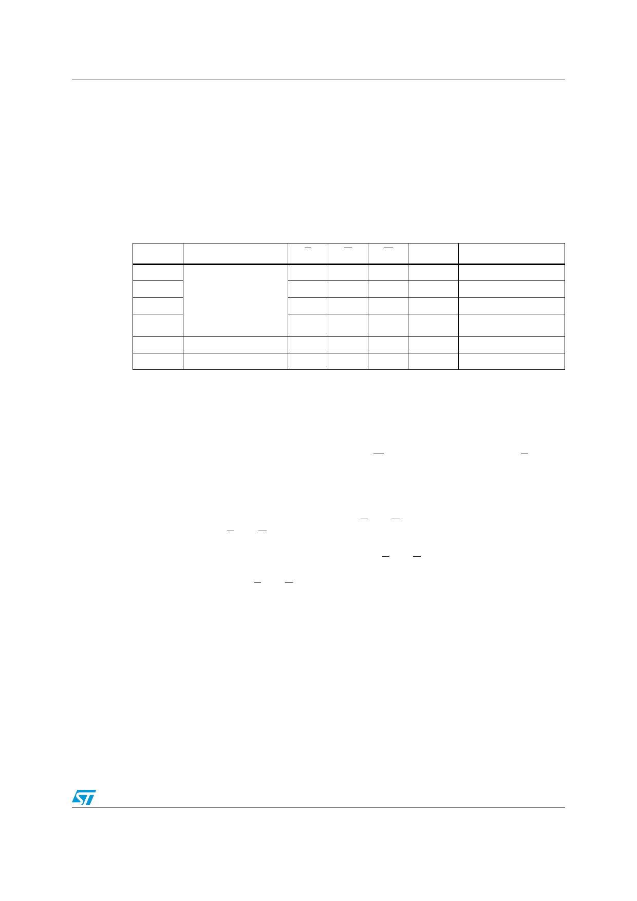
Table 2. Operating modes
Mode
VCC
E
G
W
Deselect
WRITE
READ
READ
4.75 to 5.5 V
or
4.5 to 5.5 V
or
3.0 to 3.6 V
VIH
X
X
VIL
X
VIL
VIL
VIL
VIH
VIL
VIH
VIH
Deselect VSO to VPFD (min)(1)
X
X
X
Deselect
вЙ§ VSO(1)
X
X
X
1. See Table 10 on page 15 for details.
X = VIH or VIL; VSO = battery backup switchover voltage.
DQ0-DQ7
Power
High Z
DIN
DOUT
High Z
Standby
Active
Active
Active
High Z
High Z
CMOS standby
Battery backup mode
READ mode
The M48Z128/Y/V is in the READ mode whenever W (WRITE enable) is high and E (chip
enable) is low. The device architecture allows ripple-through access of data from eight of
1,048,576 locations in the static storage array. Thus, the unique address specified by the 17
address inputs defines which one of the 131,072 bytes of data is to be accessed. Valid data
will be available at the data I/O pins within address access time (tAVQV) after the last
address input signal is stable, providing that the E and G (output enable) access times are
also satisfied. If the E and G access times are not met, valid data will be available after the
later of chip enable access time (tELQV) or output enable access time (tGLQV). The state of
the eight three-state data I/O signals is controlled by E and G. If the outputs are activated
before tAVQV, the data lines will be driven to an indeterminate state until tAVQV. If the address
inputs are changed while E and G remain low, output data will remain valid for output data
hold time (tAXQX) but will go indeterminate until the next address access.
Doc ID 2426 Rev 5
7/20
Share Link: 