MJE5740 查看數據表(PDF) - Motorola => Freescale
零件编号
产品描述 (功能)
生产厂家
MJE5740 Datasheet PDF : 6 Pages
| |||
ÎÎÎÎÎÎÎÎÎÎÎÎÎÎÎÎÎÎÎÎÎÎÎÎÎÎÎÎÎÎÎÎÎÎÎÎÎÎÎÎÎÎÎÎÎÎÎÎÎÎÎÎÎÎÎÎÎÎÎÎÎÎÎÎÎÎÎÎ MJE5740 MJE5741 MJE5742
ÎÎÎÎÎÎÎÎÎÎÎÎÎÎÎÎÎÎÎÎÎÎÎÎÎÎÎÎÎÎÎÎÎÎ ELECTRICAL CHARACTERISTICS — continued (TC = 25_C unless otherwise noted)
ÎÎÎÎÎÎÎÎÎÎÎÎÎÎÎÎÎÎÎÎÎÎÎÎÎÎÎÎÎÎÎÎÎÎ Characteristic
Symbol
Min
Typ
Max
Unit
ÎÎÎÎÎÎÎÎÎÎÎÎÎÎÎÎÎÎÎÎÎÎÎÎÎÎÎÎÎÎÎÎÎÎ ON CHARACTERISTICS (1)
ÎÎÎÎÎÎÎÎÎÎÎÎÎÎÎÎÎÎÎÎÎÎÎÎÎÎÎÎÎÎÎÎÎÎ DC Current Gain (IC = 0.5 Adc, VCE = 5 Vdc)
(IC = 4 Adc, VCE = 5 Vdc)
hFE
50
100
—
—
200
400
—
ÎÎÎÎÎÎÎÎÎÎÎÎÎÎÎÎÎÎÎÎÎÎÎÎÎÎÎÎÎÎÎÎÎÎ Collector–Emitter Saturation Voltage (IC = 4 Adc, IB = 0.2 Adc)
VCE(sat)
—
—
2
Vdc
ÎÎÎÎÎÎÎÎÎÎÎÎÎÎÎÎÎÎÎÎÎÎÎÎÎÎÎÎÎÎÎÎÎÎ Collector–Emitter Saturation Voltage (IC = 8 Adc, IB = 0.4 Adc)
—
—
3
Collector–Emitter Saturation Voltage (IC = 4 Adc, IB = 0.2 Adc, TC = 100_C)
—
—
2.2
ÎÎÎÎÎÎÎÎÎÎÎÎÎÎÎÎÎÎÎÎÎÎÎÎÎÎÎÎÎÎÎÎÎÎ Base–Emitter Saturation Voltage (IC = 4 Adc, IB = 0.2 Adc)
VBE(sat)
—
—
2.5
Vdc
ÎÎÎÎÎÎÎÎÎÎÎÎÎÎÎÎÎÎÎÎÎÎÎÎÎÎÎÎÎÎÎÎÎÎ Base–Emitter Saturation Voltage (IC = 8 Adc, IB = 0.4 Adc)
—
—
3.5
ÎÎÎÎÎÎÎÎÎÎÎÎÎÎÎÎÎÎÎÎÎÎÎÎÎÎÎÎÎÎÎÎÎÎ Base–Emitter Saturation Voltage (IC = 4 Adc, IB = 0.2 Adc, TC = 100_C)
—
—
2.4
ÎÎÎÎÎÎÎÎÎÎÎÎÎÎÎÎÎÎÎÎÎÎÎÎÎÎÎÎÎÎÎÎÎÎ Diode Forward Voltage (2) (IF = 5 Adc)
Vf
—
—
2.5
Vdc
SWITCHING CHARACTERISTICS
ÎÎÎÎÎÎÎÎÎÎÎÎÎÎÎÎÎÎÎÎÎÎÎÎÎÎÎÎÎÎÎÎÎÎ Typical Resistive Load (Table 1)
ÎÎÎÎÎÎÎÎÎÎÎÎÎÎÎÎÎÎÎÎÎÎÎÎÎÎÎÎÎÎÎÎÎÎ Delay Time
ÎÎÎÎÎÎÎÎÎÎÎÎÎÎÎÎÎÎÎÎÎÎÎÎÎÎÎÎÎÎÎÎÎÎ Rise Time
ÎÎÎÎÎÎÎÎÎÎÎÎÎÎÎÎÎÎÎÎÎÎÎÎÎÎÎÎÎÎÎÎÎÎ Storage Time
Fall Time
(VCC = 250 Vdc, IC(pk) = 6 A
v IB1 = IB2 = 0.25 A, tp = 25 µs,
Duty Cycle 1%)
ÎÎÎÎÎÎÎÎÎÎÎÎÎÎÎÎÎÎÎÎÎÎÎÎÎÎÎÎÎÎÎÎÎÎ Inductive Load, Clamped (Table 1)
td
—
0.04
—
µs
tr
—
0.5
—
µs
ts
—
8
—
µs
tf
—
2
—
µs
ÎÎÎÎÎÎÎÎÎÎÎÎÎÎÎÎÎÎÎÎÎÎÎÎÎÎÎÎÎÎÎÎÎÎ Voltage Storage Time
ÎÎÎÎÎÎÎÎÎÎÎÎÎÎÎÎÎÎÎÎÎÎÎÎÎÎÎÎÎÎÎÎÎÎ Crossover Time
(IC(pk) = 6 A, VCE(pk) = 250 Vdc
IB1 = 0.06 A, VBE(off) = 5 Vdc)
ÎÎÎÎÎÎÎÎÎÎÎÎÎÎÎÎÎÎÎÎÎÎÎÎÎÎÎÎÎÎÎÎÎÎ (1) Pulse Test: Pulse Width 300 µs, Duty Cycle = 2%.
tsv
—
4
—
µs
tc
—
2
—
µs
(2) The internal Collector–to–Emitter diode can eliminate the need for an external diode to clamp inductive loads. Tests have shown that the
(2) Forward Recovery Voltage (Vf) of this diode is comparable to that of typical fast recovery rectifiers.
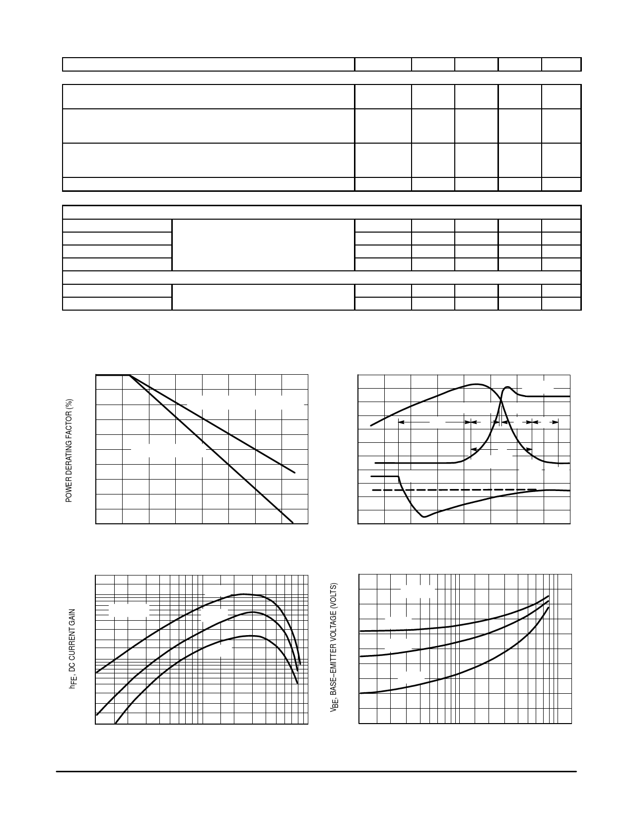
TYPICAL CHARACTERISTICS
100
IC(pk)
VCE(pk)
80
SECOND BREAKDOWN DERATING
90% VCE(pk) 90% IC
IC
tsv
trv
tfi
tti
60
THERMAL DERATING
40
VCE
IB
90% IB1
tc
10% VCE(pk)
10%
IC(pk) 2% IC
20
0
0 20 40 60 80 100 120 140 160
TC, CASE TEMPERATURE (°C)
Figure 1. Power Derating
2000
1000
VCE = 5 V
150°C
+ 25°C
– 55°C
100
10
0.1
1
2
5
10
IC, COLLECTOR CURRENT (AMPS)
Figure 3. DC Current Gain
TIME
Figure 2. Inductive Switching Measurements
2.4
2.2
hFE = 20
2
1.8
– 55°C
1.6
1.4
+ 25°C
1.2
1
+150°C
0.8
0.6
0.4
0.2
0.5
1
2
5
10
IC, COLLECTOR CURRENT (AMPS)
Figure 4. Base–Emitter Voltage
2
Motorola Bipolar Power Transistor Device Data
Share Link: 