DS1994L-F5 查看數據表(PDF) - Dallas Semiconductor -> Maxim Integrated
零件编号
产品描述 (功能)
生产厂家
DS1994L-F5 Datasheet PDF : 22 Pages
| |||
DS1994
7 DSEL Delay Select Bit
This bit selects the delay that it takes for the cycle counter and the interval timer (in auto mode) to see a
transition on the data line. When this bit is set to a logic 1, the delay time is 123 ± 2ms. This delay allows
communication on the data line without starting or stopping the interval timer and without incrementing
the cycle counter. When this bit is set to a logic 0, the delay time is 3.5 ± 0.5ms.
MEMORY FUNCTION COMMANDS
The Memory Function Flowchart (Figure 6) describes the protocols necessary for accessing the memory.
An example follows the flowchart. Three address registers are provided as shown in Figure 5. The first
two registers represent a 16-bit target address (TA1, TA2). The third register is the ending offset/data
status Byte (E/S).
The target address points to a unique Byte location in memory. The first 5 bits of the target address
(T4:T0) represent the Byte offset within a page. This Byte offset points to one of 32 possible Byte
locations within a given page. For instance, 00000b points to the first Byte of a page where as 11111b
would point to the last Byte of a page.
The third register (E/S) is a read only register. The first 5 bits (E4:E0) of this register are called the
ending offset. The ending offset is a Byte offset within a page (1 of 32 Bytes). Bit 5 (PF) is the partial
Byte flag. Bit 6 (OF) is the overflow flag. Bit 7 (AA) is the authorization accepted flag.
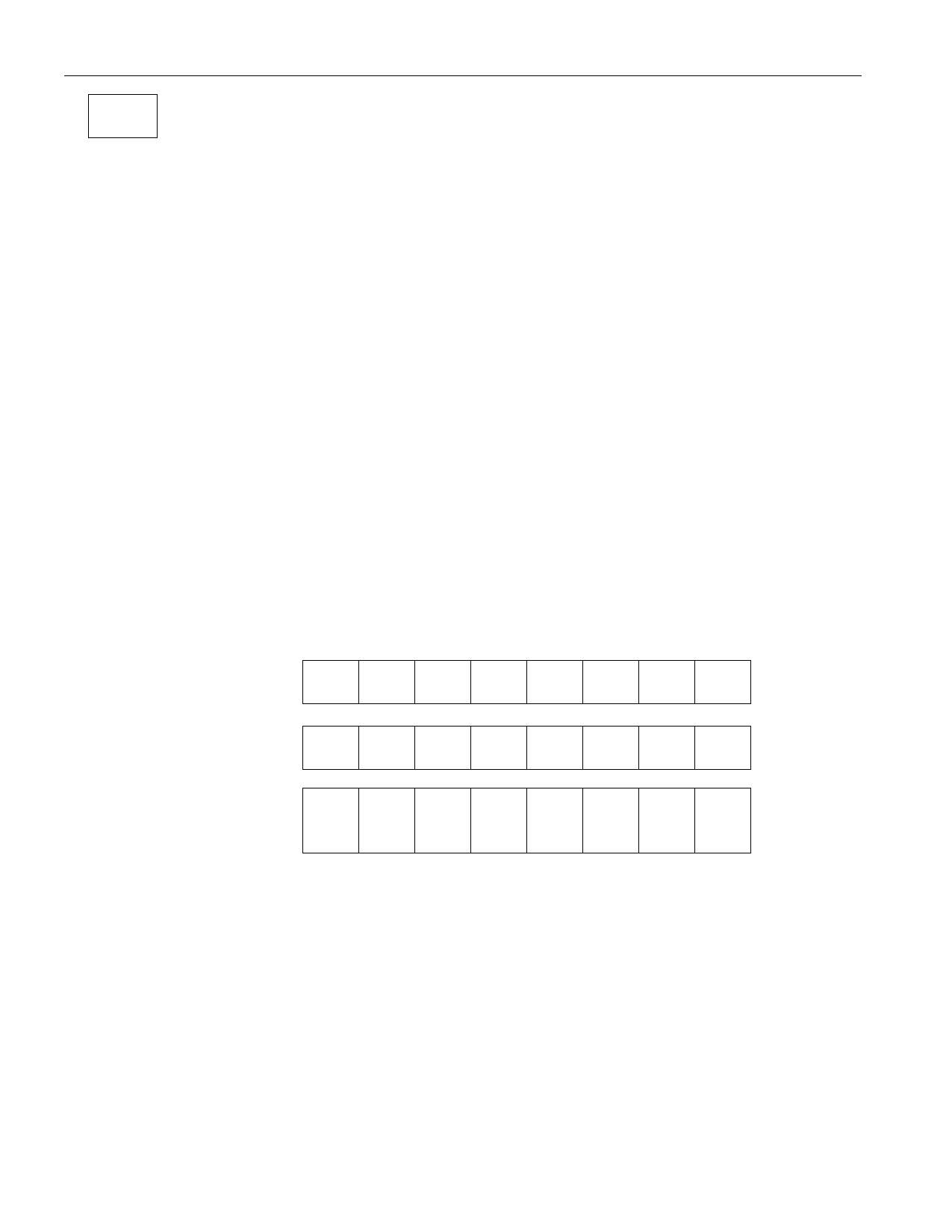
Figure 5. ADDRESS REGISTERS
TARGET ADDRESS (TA1)
76543210
T7 T6 T5 T4 T3 T2 T1 T0
TARGET ADDRESS (TA2) T15 T14 T13 T12 T11 T10 T9 T8
ENDING ADDRESS WITH
DATA STATUS (E/S)
AA OF PF E4 E3 E2 E1 E0
(READ ONLY)
Write Scratchpad Command [0Fh]
After issuing the write scratchpad command, the user must first provide the 2-Byte target address,
followed by the data to be written to the scratchpad. The data is written to the scratchpad starting at the
Byte offset (T4:T0). The ending offset (E4:E0) is the Byte offset at which the host stops writing data. The
maximum ending offset is 11111b (31d). If the host attempts to write data past this maximum offset, the
overflow flag (OF) is set and the remaining data is ignored. If the user writes an incomplete Byte and an
overflow has not occurred, the partial Byte flag (PF) is set.
Read Scratchpad Command [AAh]
This command can be used to verify scratchpad data and target address. After issuing the read scratchpad
command, the user can begin reading. The first two Bytes are the target address. The next Byte is the
8 of 22
Share Link: 