S15 查看數據表(PDF) - Union Semiconductor, Inc.
零件编号
产品描述 (功能)
生产厂家
S15 Datasheet PDF : 5 Pages
| |||
SM12/SM15
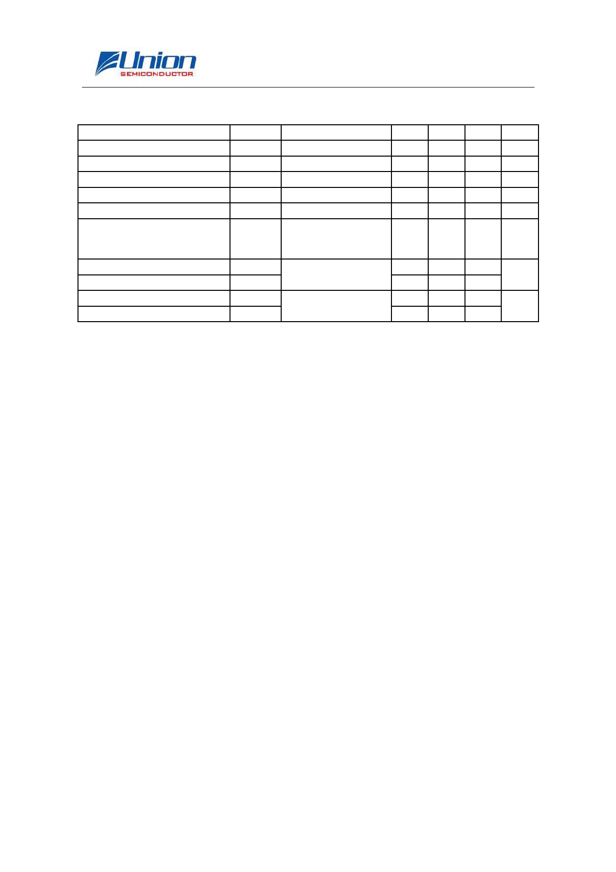
Electrical Characteristics (SM15)
Parameter
Reverse Stand-Off Voltage
Reverse Breakdown Voltage
Reverse Leakage Current
Clamping Voltage
Peak Pulse Current
Junction Capacitance
Reverse Dynamic Resistance
Forward Dynamic Resistance
Reverse Dynamic Resistance
Forward Dynamic Resistance
Symbol
Conditions
Min Typ Max Unit
VRWM
15 V
VBR
IT=1mA
16.7
18.7 V
IR
VRWM=15V, T=25°C
1 μA
VC
IPP=5.9A, tp=8/20μs
23 V
IPP
CJ
Rdyn,rev
Rdyn,fwd
tp=8/20μs
Pin 1 to 3 and
Pin 2 to 3,
VR=0V, f=1MHz
IPP<2A
5.9 A
20 30 pF
1.12
Ω
0.81
Rdyn,rev
Rdyn,fwd
IPP>2A
0.92
Ω
0.42
Detailed Description
Device Connection Options
SM12/SM15 is designed to protect one bidirectional or two unidirectional data or I/O lines
operating at 12V/15V. Connection options are as follows: Bidirectional: Pin 1 is connected to the
data line and pin 2 is connected to ground (Since the device is symmetrical, these connections
may be reversed). The ground connection should be made directly to a ground plane. The path
length should be kept as short as possible to minimize parasitic inductance. Pin 3 is not connected.
Unidirectional: Data lines are connected to pin 1 and pin 2. Pin 3 is connected to ground. For best
results, this pin should be connected directly to a ground plane on the board. The path length
should be kept as short as possible to minimize parasitic inductance.
Circuit Board Layout Recommendations for Suppression of ESD
Good circuit board layout is critical for the suppression of fast rise-time transients such as ESD.
The following guidelines are recommended (Refer to application note SI99-01 for more detailed
information): Place the TVS near the input terminals or connectors to restrict transient coupling.
Minimize the path length between the TVS and the protected line. Minimize all conductive loops
including power and ground loops. The ESD transient return path to ground should be kept as
short as possible. Never run critical signals near board edges. Use ground planes whenever
possible.
Matte Tin Lead Finish
Matte tin has become the industry standard lead-free replacement for SnPb lead finishes. A matte
tin finish is composed of 100% tin solder with large grains. Since the solder volume on the leads
is small compared to the solder paste volume that is placed on the land pattern of the PCB, the
reflow profile will be determined by the requirements of the solder paste. Therefore, these devices
are compatible with both lead-free and SnPb assembly techniques. In addition, unlike other
lead-free compositions, matte tin does not have any added alloys that can cause degradation of the
solder joint.
________________________________________________________________________
http://www.union-ic.com Rev.03 May.2016
3/5
Share Link: 