FM1608B(2013) 查看數據表(PDF) - Cypress Semiconductor
零件编号
产品描述 (功能)
生产厂家
FM1608B Datasheet PDF : 14 Pages
| |||
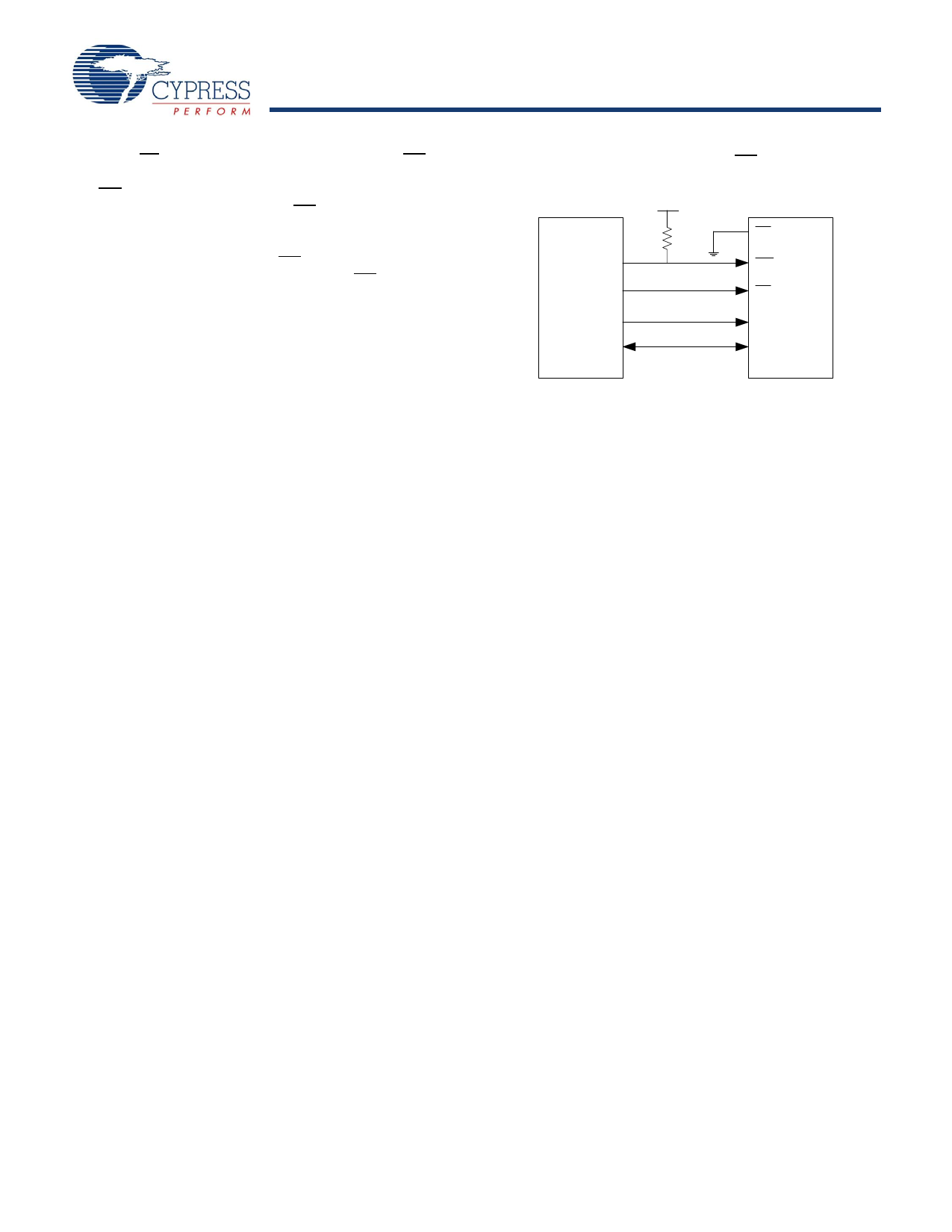
FM1608B – 64Kb Bytewide 5V F-RAM
Electrical Specifications
Absolute Maximum Ratings
Symbol
Description
VDD
Power Supply Voltage with respect to VSS
VIN
Voltage on any pin with respect to VSS
TSTG
TLEAD
VESD
Storage Temperature
Lead Temperature (Soldering, 10 seconds)
Electrostatic Discharge Voltage
- Human Body Model (AEC-Q100-002 Rev. E)
- Charged Device Model (AEC-Q100-011 Rev. B)
- Machine Model (AEC-Q100-003 Rev. E)
Package Moisture Sensitivity Level
Ratings
-1.0V to +7.0V
-1.0V to +7.0V
and VIN < VDD+1.0V
-55 C to + 125 C
260 C
4kV
1.25kV
300V
MSL-2
Stresses above those listed under Absolute Maximum Ratings may cause permanent damage to the device. This is a stress rating
only, and the functional operation of the device at these or any other conditions above those listed in the operational section of this
specification is not implied. Exposure to absolute maximum ratings conditions for extended periods may affect device reliability.
DC Operating Conditions (TA = -40 C to + 85 C, VDD = 4.5V to 5.5V unless otherwise specified)
Symbol Parameter
Min
Typ
Max
VDD
IDD
ISB1
ISB2
ILI
ILO
VIH
VIL
VOH1
VOH2
VOL1
VOL2
Power Supply
VDD Supply Current
Standby Current (TTL)
Standby Current (CMOS )
Input Leakage Current
Output Leakage Current
Input High Voltage
Input Low Voltage
Output High Voltage (IOH = -2 mA)
Output High Voltage (IOH = -100 A)
Output Low Voltage (IOL = 4.2 mA)
Output Low Voltage (IOL = 150 A)
4.5
5.0
5.5
-
15
-
1.8
25
50
-
1
-
1
2.0
VDD+0.3
-0.3
0.8
2.4
VDD-0.2
0.4
0.2
Notes
1. VDD = 5.5V, /CE cycling at minimum cycle time. All inputs at CMOS levels, all outputs unloaded.
2. VDD = 5.5V, /CE at VIH, All other pins at TTL levels.
3. VDD = 5.5V, /CE at VIH, All other pins at CMOS levels (0.2V or VDD-0.2V).
4. VIN, VOUT between VDD and VSS.
Units
V
mA
mA
A
A
A
V
V
V
V
V
V
Notes
1
2
3
4
4
Document Number: 001-86211 Rev. *A
Page 6 of 14
Share Link: 