FM24C04B-G 查看數據表(PDF) - Cypress Semiconductor
零件编号
产品描述 (功能)
生产厂家
FM24C04B-G Datasheet PDF : 13 Pages
| |||
AC Test Conditions
Input Pulse Levels
Input rise and fall times
Input and output timing levels
0.1 VDD to 0.9 VDD
10 ns
0.5 VDD
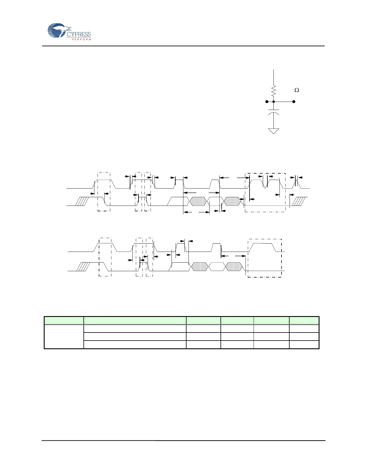
Diagram Notes
All start and stop timing parameters apply to both read and write cycles.
Clock specifications are identical for read and write cycles. Write timing
parameters apply to slave address, word address, and write data bits.
Functional relationships are illustrated in the relevant datasheet sections.
These diagrams illustrate the timing parameters only.
FM24C04B
Equivalent AC Load Circuit
5.5V
Output
1700
100 pF
Read Bus Timing
SCL
tR
tHIGH
` tF
tLOW
tSP
tSP
SDA
tSU:SDA
tBUF
1/fSCL
tHD:DAT
tSU:DAT
Start
Stop Start
tAA
tDH
Acknowledge
Write Bus Timing
SCL
SDA
tSU:STO
tHD:STA
Start
Stop Start
tHD:DAT
tSU:DAT
tAA
Acknowledge
Data Retention
Symbol
Parameter
TDR
@ +85ºC
@ +80ºC
@ +75ºC
Min
Max
Units
Notes
10
-
Years
19
-
Years
38
-
Years
Document Number: 001-84446 Rev. *A
Page 10 of 13
Share Link: 