VN820-B513TR(2003) 查看數據表(PDF) - STMicroelectronics
零件编号
产品描述 (功能)
生产厂家
VN820-B513TR Datasheet PDF : 34 Pages
| |||
VN820 / VN820SO / VN820SP / VN820-B5 / VN820PT
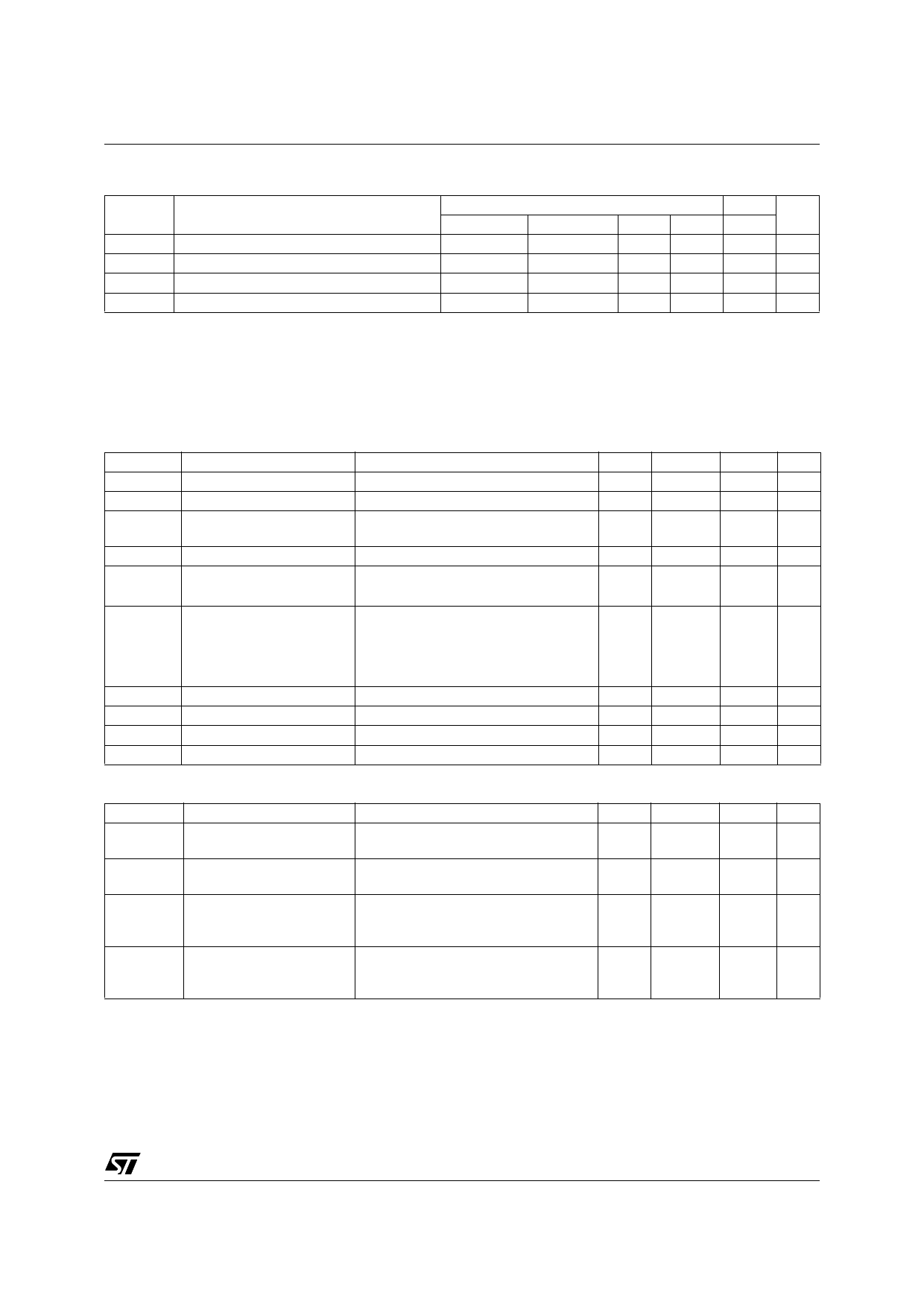
THERMAL DATA
Symbol
Rthj-case
Rthj-lead
Rthj-amb
Parameter
Value
PowerSO-10™ PENTAWATT P2PAK SO-16L PPAK Unit
Thermal Resistance Junction-case Max
1.9
1.9
1.9
-
1.9 °C/W
Thermal Resistance Junction-lead Max
-
-
-
15
- °C/W
Thermal Resistance Junction-ambient Max 51.9 (*)
61.9 (*) 51.9 (*) 65 (**) 76.9 (*) °C/W
(*) When mounted on a standard single-sided FR-4 board with 0.5cm2 of Cu (at least 35µm thick).
(**) When mounted on FR4 printed circuit board with 0.5cm2 of Cu (at least 35µ thick) connected to all VCC pins.
ELECTRICAL CHARACTERISTICS (8V<VCC<36V; -40°C<Tj<150°C unless otherwise specified)
POWER
Symbol
Parameter
Test Conditions
Min
Typ
Max Unit
VCC
VUSD
VUSDhyst
Operating Supply Voltage
Undervoltage Shut-down
Undervoltage Shut-down
hysteresis
5.5
13
3
4
36
V
5.5
V
0.5
V
VOV Overvoltage Shut-down
36
V
RON On State Resistance
IOUT=3A; Tj=25°C; VCC>8V
IOUT=3A; VCC>8V
40 mΩ
80 mΩ
Off State; VCC=13V; VIN=VOUT=0V
10
25 µA
IS
Supply Current
Off State; VCC=13V; VIN=VOUT=0V;
Tj=25°C
10
20 µA
On State; VCC=13V; VIN=5V; IOUT=0A
2
3.5 mA
IL(off1) Off State Output Current VIN=VOUT=0V
0
IL(off2) Off State Output Current VIN=0V; VOUT=3.5V
-75
IL(off3) Off State Output Current VIN=VOUT=0V; Vcc=13V; Tj =125°C
IL(off4) Off State Output Current VIN=VOUT=0V; Vcc=13V; Tj =25°C
50 µA
0
µA
5
µA
3
µA
SWITCHING (VCC=13V)
Symbol
Parameter
td(on) Turn-on Delay Time
td(off)
Turn-off Delay Time
dVOUT/dt(on) Turn-on Voltage Slope
dVOUT/dt(off) Turn-off Voltage Slope
Test Conditions
RL=4.3Ω from VIN rising edge to
VOUT=1.3V
RL=4.3Ω from VIN falling edge to
VOUT=11.7V
RL=4.3Ω from VOUT=1.3 to
VOUT=10.4V
RL=4.3Ω from VOUT=11.7 to
VOUT=1.3V
Min
Typ
Max Unit
30
µs
30
See
relative
diagram
See
relative
diagram
µs
V/µs
V/µs
INPUT PIN
Symbol
VIL
IIL
VIH
IIH
VI(hyst)
Parameter
Input Low Level
Low Level Input Current
Input High Level
High Level Input Current
Input Hysteresis Voltage
VICL
Input Clamp Voltage
Test Conditions
VIN=1.25V
VIN=3.25V
IIN=1mA
IIN=-1mA
Min
Typ
Max Unit
1.25 V
1
µA
3.25
V
10
µA
0.5
V
6
6.8
8
V
-0.7
V
3/34
1
Share Link: 