ISL8201M 查看數據表(PDF) - Renesas Electronics
零件编号
产品描述 (功能)
生产厂家
ISL8201M Datasheet PDF : 16 Pages
| |||
ISL8201M
Applications Information
The typical ISL8201M application schematic for input voltage
+5V or +12V is shown in Figure 11. External component
selection is primarily determined by the maximum load current
and input/output voltage.
Programming the Output Voltage
The ISL8201M has an internal 0.6V ±1.5% reference voltage.
Programming the output voltage requires a dividing resistor
(RFB). The output voltage can be calculated as shown in
Equation 1:
VOUT
=
0.6
1
+
-9-R--.--7-F--6-B---k-
(EQ. 1)
Note: ISL8201M has integrated 9.76k resistance into the
module (dividing resistor for top side). The resistance
corresponding to different output voltages is as shown in
Table 1:
TABLE 1. RESISTANCE TO OUTPUT VOLTAGES
VOUT
RFB
VOUT
RFB
0.6V
open
1.8V
4.87k
1.05V
13k
2.5V
3.09k
1.2V
9.76k
3.3V
2.16k
1.5V
6.49k
5V
1.33k
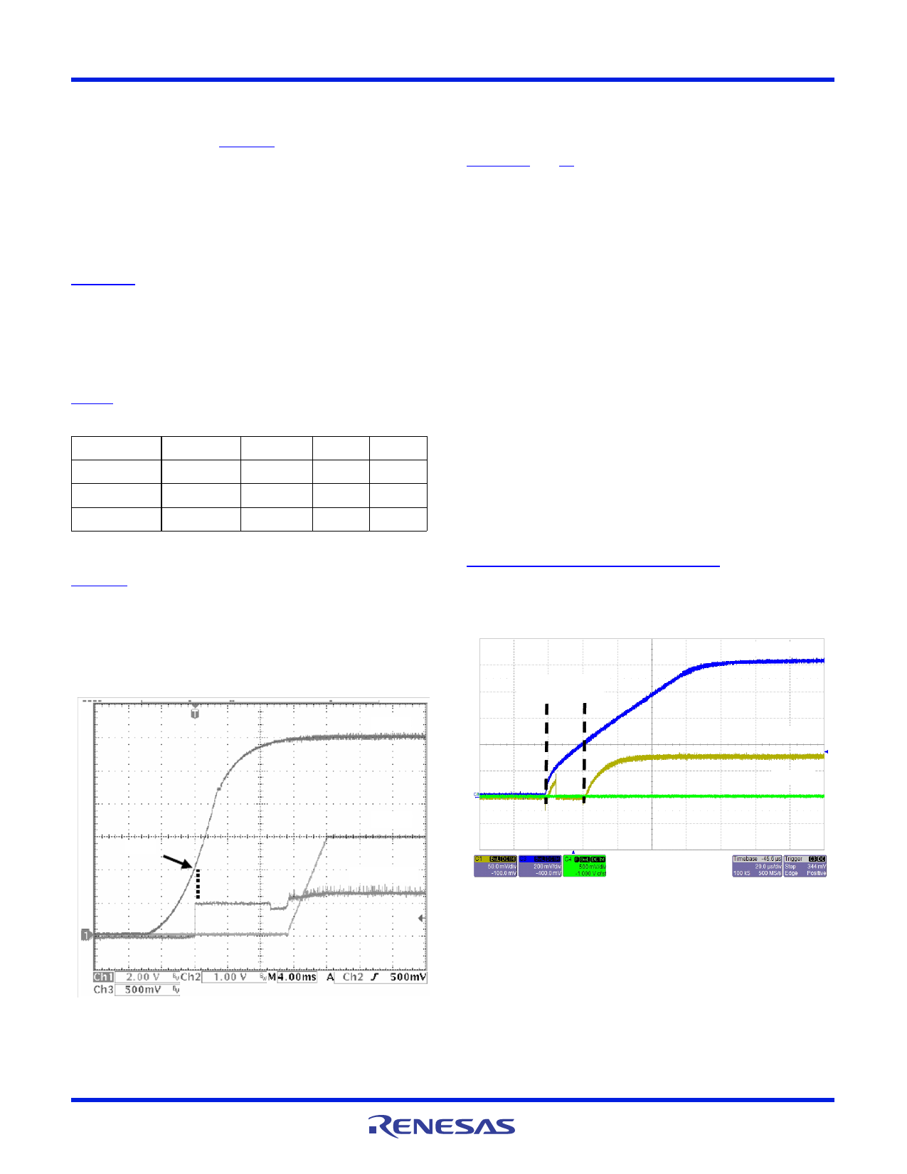
Initialization (POR and OCP Sampling)
Figure 13 shows a start-up waveform of ISL8201M. The
power-on-reset (POR) function continually monitors the bias
voltage at the PVCC pin. Once the rising POR threshold has
exceeded 4V (VPORR nominal), the POR function initiates the
overcurrent protection (OCP) sample and hold operation (while
COMP/EN is ~1V). When the sampling is complete, VOUT
begins the soft-start ramp.
PVCC
If the COMP/EN pin is held low during power-up, the
initialization will be delayed until the COMP/EN is released and
its voltage rises above the VENDIS trip point.
Figures 14 and 15 show a typical power-up sequence in more
detail. The initialization starts at t0, when either PVCC rises
above VPORR, or the COMP/EN pin is released (after POR).
The COMP/EN will be pulled up by an internal 20µA current
source, however, the timing will not begin until the COMP/EN
exceeds the VENDIS trip point (at t1). The external capacitance
of the disabling device, as well as the compensation
capacitors, will determine how quickly the 20µA current source
will charge the COMP/EN pin. With typical values, it should
add a small delay compared to the soft-start times. The
COMP/EN will continue to ramp to ~1V.
From t1, there is a nominal 6.8ms delay, which allows the
PVCC pin to exceed 6.5V (if rising up towards 12V), so that the
internal bias regulator can turn on cleanly. At the same time,
the ISET pin is initialized by disabling the low-side gate driver
and drawing ISET (nominal 21.5µA) through RSETI. This sets up
a voltage that will represent the ISET trip point. At t2, there is a
variable time period for the OCP sample and hold operation
(0.0ms to 3.4ms nominal; the longer time occurs with the
higher overcurrent setting). The sample and hold uses a digital
counter and DAC to save the voltage, so the stored value does
not degrade, as long as the PVCC is above VPORR (See
“Overcurrent Protection (OCP)” on page 10 for more details on
the equations and variables). Upon the completion of sample
and hold at t3, the soft-start operation is initiated, and the
output voltage ramps up between t4 and t5.
COCMOMPP/E/ENN
T0t0 Tt11
ISET ISET
VOUT VOUT
VOUT
~4V
COMP/EN
FIGURE 14. ISET AND SOFT-START OPERATION
FIGURE 13. POR AND SOFT-START OPERATION
FN6657 Rev 3.00
October 28, 2014
Page 8 of 16
Share Link: 