FPF1005 查看數據表(PDF) - ON Semiconductor
零件编号
产品描述 (功能)
生产厂家
FPF1005 Datasheet PDF : 9 Pages
| |||
Description of Operation
The FPF1005 & FPF1006 are low RDS(ON) P-Channel load
switches with controlled turn-on. The core of each device is a
55mΩ P-Channel MOSFET and a controller capable of
functioning over a wide input operating range of 1.2-5.5V. The
ON pin, an active HI TTL compatible input, controls the state of
the switch. The FPF1006 contains a 120Ω on-chip load resistor
for quick output discharge when the switch is turned off.
However, VOUT pin of FPF1006 should not be connected
directly to the battery source due to the discharge mechanism of
the load switch.
Application Information
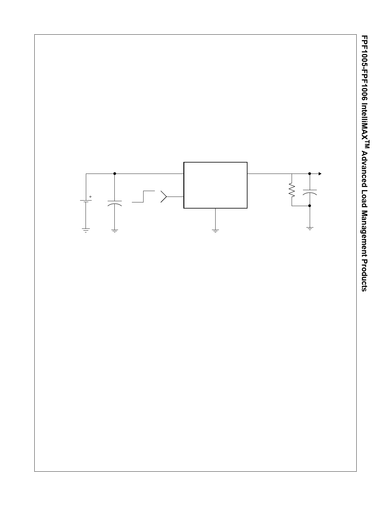
Typical Application
VIN
VOUT
CIN
VIN = 3.3V
FPF1005/6
RL
OFF ON
ON
-
GND
VON = 3.3V
Input Capacitor
To limit the voltage drop on the input supply caused by transient
in-rush currents when the switch turns-on into a discharged load
capacitor or short-circuit, a capacitor needs to be placed
between VIN and GND. A 1µF ceramic capacitor, CIN, placed
close to the pins is usually sufficient. Higher values of CIN can
be used to further reduce the voltage drop during higher current
application.
Output Capacitor
A 0.1µF capacitor, COUT, should be placed between VOUT and
GND. This capacitor will prevent parasitic board inductance
from forcing VOUT below GND when the switch turns-off. Due to
the integral body diode in the PMOS switch, a CIN greater than
COUT is highly recommended. A COUT greater than CIN can
cause VOUT to exceed VIN when the system supply is removed.
This could result in current flow through the body diode from
VOUT to VIN.
Board Layout
For best performance, all traces should be as short as possible.
To be most effective, the input and output capacitors should be
placed close to the device to minimize the effects that parasitic
trace inductances may have on normal and short-circuit
operation. Using wide traces or large copper planes for all pins
(VIN, VOUT, ON and GND) will help minimize the parasitic
electrical effects along with minimizing the case to ambient
thermal impedance.
COUT
www.onsemi.com
7
Share Link: 