FPF1005 查看數據表(PDF) - ON Semiconductor
零件编号
产品描述 (功能)
生产厂家
FPF1005 Datasheet PDF : 9 Pages
| |||
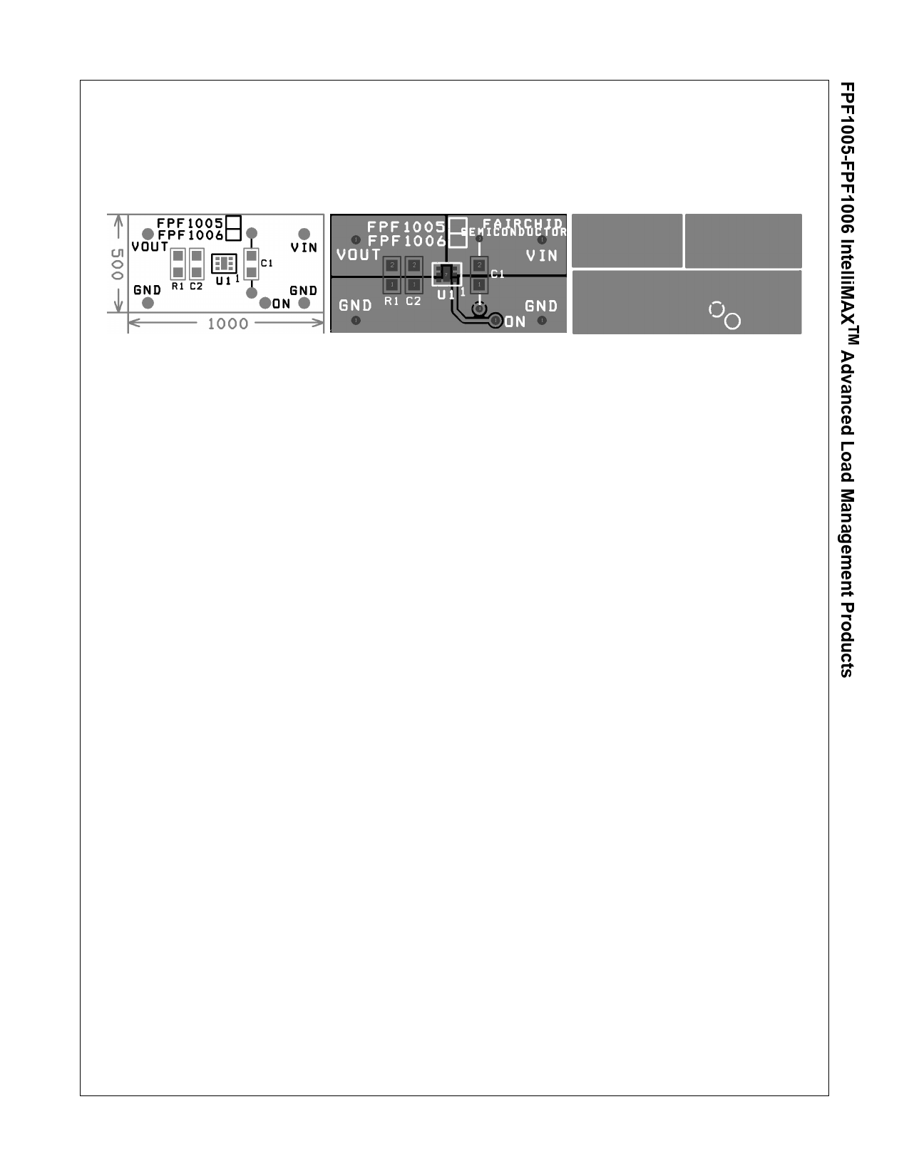
Evaluation Board Layout
FPF1005/6 Demo board has the components and circuitry to demonstrate the load switch functions. Thermal performance of the load
switch can be improved significantly by connecting the middle pad (pin 7) to the GND area of the PCB.
Figure 19. Demo board silk screen top
and component assembly drawing.
Figure 20. Demo board top and surface
mount top layers view.(Pin 7 is connected
to GND).
Figure 21. Demo board bottom layer view.
www.onsemi.com
8
Share Link: 