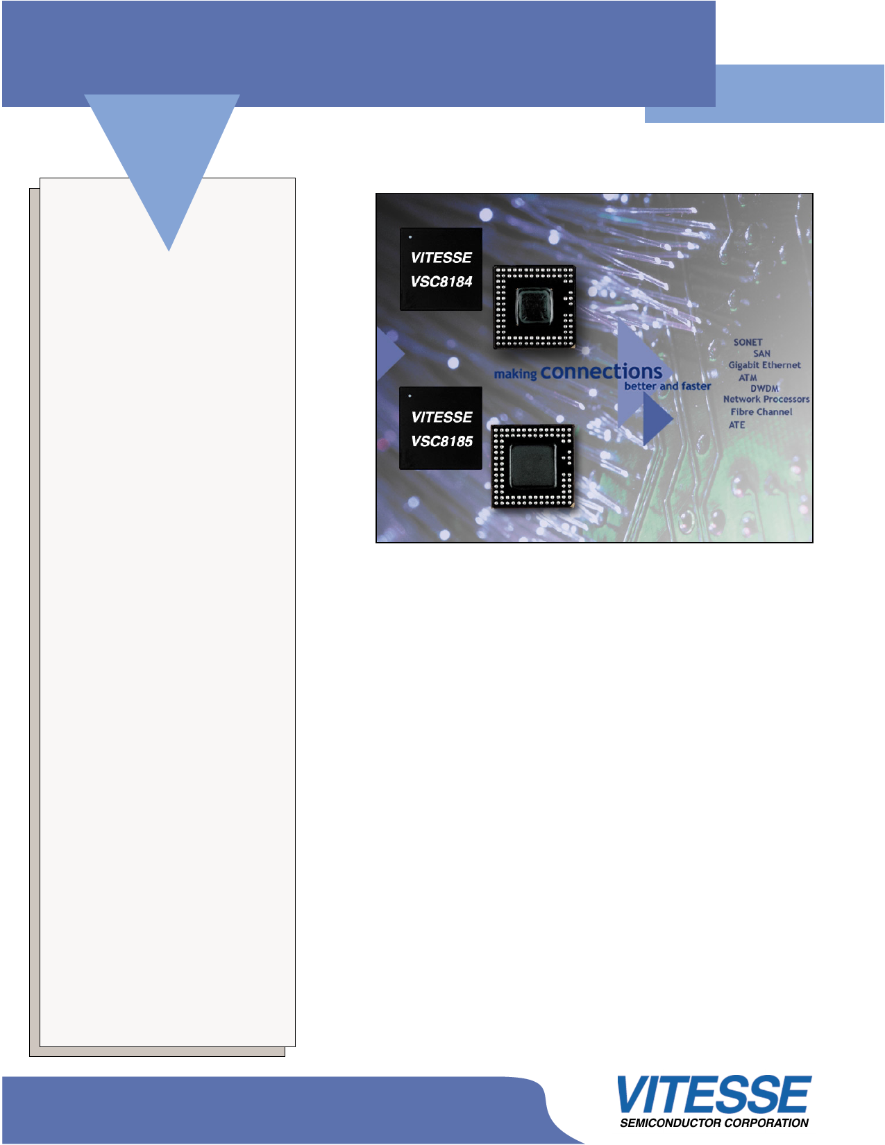
VSC8185 查看數據表(PDF) - Vitesse Semiconductor
零件编号
产品描述 (功能)
生产厂家
VSC8185 Datasheet PDF : 2 Pages
| |||

11.5-12.5Gb/s 16:1 Multiplexer with Clock Generator
Physical
Layer
Products
VSC8185
Product Brief
Features:
• High Speed Operation Up to
12.5Gb/s with Integrated Clock
Multiplier Unit
• High-Speed Output Clock
• Narrow Clock-to-Data Skew
Range
• Superior Data Output Eyes
• Low Power 1.7W (Typ)
• +3.3V Single Supply
• Continuous Tuning Operation
from 11.5 to 12.5Gb/s Rates
• 180/195 or 719/781 MHz
Reference Clock Input
• Reliable 90-Ball TBGA Package
• Up to 90°C Case Temperature
Specifications:
• 11.5 to 12.5Gb/s Continuous
Operation
• Data Output Voltage Swing:
500 mV (min)
• Data Output Rise/Fall:
25 ps (Typ)
• High Speed Clock Voltage
Swing: 400 mV (min)
• +/- 15 ps Clock-to-Data Skew
Range Over Temperature
• Supply Voltage: 3.3V (Typ)
• Total Power Dissipation:
1.7W (Typ)
• Operating Temperature Range:
0°C to +90°C (case)
• 15x15mm Low Profile 90 Ball
TBGA (Taped BGA) Package
General Description
The VSC8185 consists of a 16:1 Mul-
tiplexer and a clock generator for use
in SONET STS-192 / SDH STM-64
systems. The 16:1 Multiplexer accepts
16 parallel low voltage differential
swing (LVDS) inputs (D[0:15]±) and
(PARITY±) at a data rate of 718.8 to
781.3 Mb/s. This parallel data stream
is then serialized into a 11.5Gb/s to
12.5Gb/s output (DOUT±). The clock
generator creates the 11.5GHz to
12.5GHz clock signal used to re-time
the transmitted serialized data. The
clock generator requires a 180-
195MHz or 719-781MHz PECL refer-
ence clock input (REFCK±). To ease
timing constraints on the parallel inter-
face, a 16 bit wide FIFO is included. A
high speed clock output (COUT±) is
provided that is synchronized to the
high speed serial data output. A divide-
by-16 or divide-by-64 LVDS clock out-
put (CK16_64±) is available for use as
a clock input to the data source of the
parallel inputs (D[0:15]±) and (PAR-
ITY±). Additional features include par-
ity bit (PARITY±) that is clocked in with
the 16-bit parallel data. Bit Order Swap
(BITORDER) and Data Polarity Invert
(DINVERT). To assist in monitoring
device operation a Loss-of-Lock
(LOLN) alarm and internal temperature
diode are included. The device is pack-
aged in a modified 90-ball, Ball Grid
Array (BGA).
www.vitesse.com Physical Layer Products