VSC8185 查看數據表(PDF) - Vitesse Semiconductor
零件编号
产品描述 (功能)
生产厂家
VSC8185 Datasheet PDF : 2 Pages
| |||
11.5-12.5Gb/s 16:1 Multiplexer with Clock Generator
Product Brief
VSC8185
Physical
Layer
Products
Benefits:
• Provides High-speed Output
Clock for RZ and Re-timed
Laser Driver Applications
• Provides Lowest Power Solution
in its Performance Class
• Pin-compatible Path to 9.9 to
10.7Gb/s Product (VSC8175)
• Integrated PLL Based Clock
Generator
• True LVDS Parallel Data
Interface
• Thermal Expansion of TBGA
Package is Matched to the PC
Board for High Reliability
• Input FIFO to Simplify Parallel
Interface Timing
• Data Polarity Invert and Bit
Order Swap for Ease of Layout
Applications:
• Advanced Forward Error
Correction (FEC)
• Return-to-Zero Transmission
Applications
• Re-Timing Laser Drivers
• Ultra-Long Haul Systems
• SONET/SDH Networking
• DWDM Systems
• Telecommunications Transmis-
sion Systems
• Test Equipment
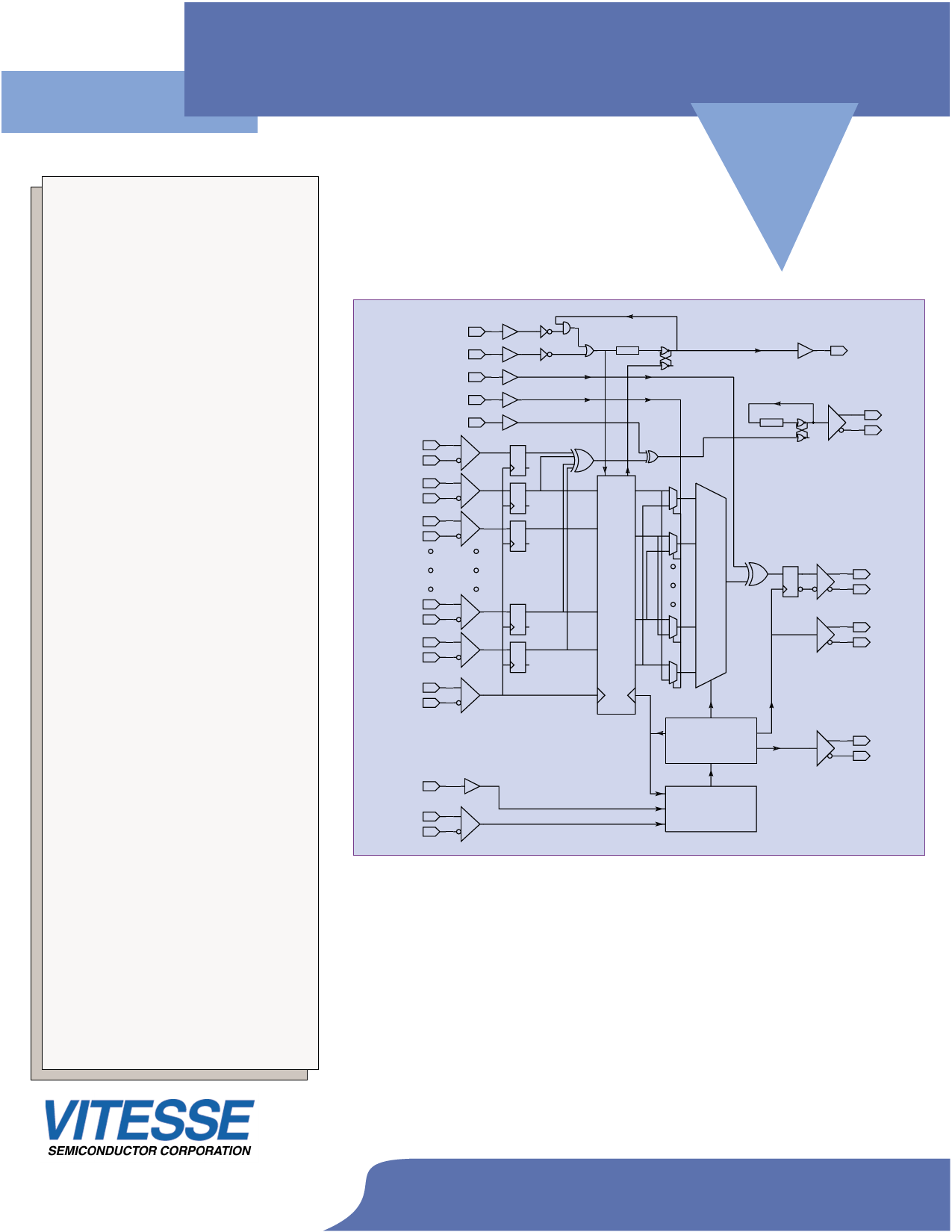
VSC8185 Block Diagram
AUTORSTN
RESETN
DINVERT
BITORDER
PARSENSE
PARITY+
PARITY-
D0+
D0-
D1+
D1-
D14+
D14-
D15+
D15-
DCK+
DCK-
REFSEL
REFCK+
REFCK-
DELAY
RST
OVR
FIFO
CK/16
DELAY
OVERFLOW
DINVALID+
DINVALID-
16:1
DOUT+
DOUT-
COUT+
COUT-
TIMING
GENERATOR
11.5G-12.5G
PLL
CK16_64+
CK16_64-
719MHz/180MHz
www.vitesse.com
For more information on Vitesse Products visit the Vitesse web site
at www.vitesse.com or contact Vitesse Sales at (800) VITESSE or
sales@vitesse.com
© Copyright 2000 Vitesse Semiconductor Corporation
and the Vitesse logo are all registered trademarks
of Vitesse Semiconductor Corp;oration
Share Link: 