ISL59451 查看數據表(PDF) - Renesas Electronics
零件编号
产品描述 (功能)
生产厂家
ISL59451 Datasheet PDF : 17 Pages
| |||
ISL59451
Absolute Maximum Ratings (TA = +25°C)
Supply Voltage (V+ to GND) . . . . . . . . . . . . . . . . . . . . . . . . . . . 5.5V
Input Voltage to GND. . . . . . . . . . . . . . . . . .GND - 0.5V to V+ +0.5V
Voltage between HIZ, CLAMP, AV2, REF_ and GND
. . . . . . . . . . . . . . . . . . . . . . . . . . . . . . . . . . . . GND - 0.5;V+ +0.5V
Supply Turn-on Slew Rate . . . . . . . . . . . . . . . . . . . . . . . . . . . 1V/µs
Digital and Analog Input Current (Note 1) . . . . . . . . . . . . . . . . 50mA
Output Current (Continuous) . . . . . . . . . . . . . . . . . . . . . . . . . . 50mA
ESD Rating
Human Body Model (Per MIL-STD-883 Method 3015.7). . . .2500V
Machine Model . . . . . . . . . . . . . . . . . . . . . . . . . . . . . . . . . . .300V
Thermal Information
Storage Temperature Range . . . . . . . . . . . . . . . . . . -65°C to +150°C
Ambient Operating Temperature . . . . . . . . . . . . . . . . -40°C to +85°C
Operating Junction Temperature . . . . . . . . . . . . . . . -40°C to +125°C
Power Dissipation . . . . . . . . . . . . . . . . . . . . . . . . . . . . . .See Curves
Pb-free reflow profile . . . . . . . . . . . . . . . . . . . . . . . . . .see link below
http://www.intersil.com/pbfree/Pb-FreeReflow.asp
CAUTION: Do not operate at or near the maximum ratings listed for extended periods of time. Exposure to such conditions may adversely impact product reliability and
result in failures not covered by warranty.
NOTE:
1. If an input signal is applied before the supplies are powered up, the input current must be limited to these maximum values.
2. Parts are 100% tested at +25°C. Over-temperature limits established by characterization and are not production tested.
IMPORTANT NOTE: All parameters having Min/Max specifications are guaranteed. Typical values are for information purposes only. Unless otherwise noted, all tests
are at the specified temperature and are pulsed tests, therefore: TJ = TC = TA
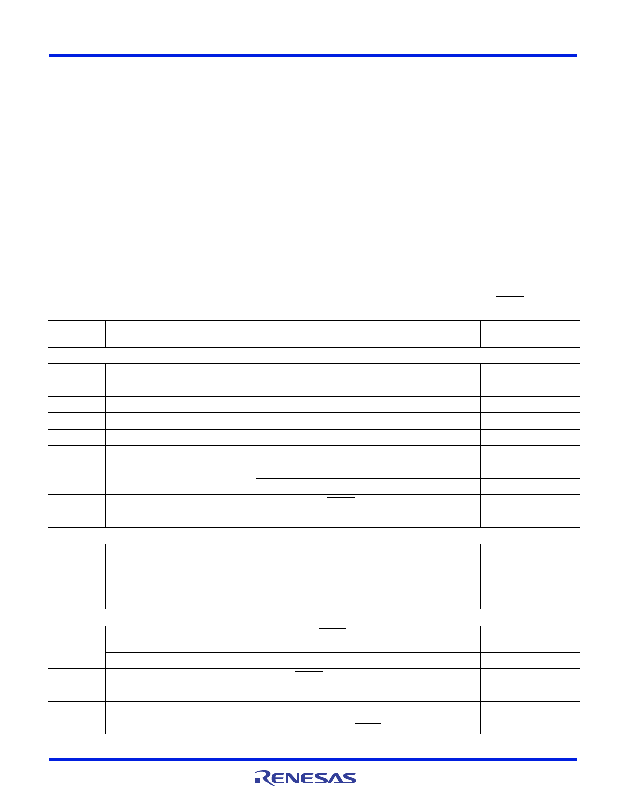
Electrical Specifications V+ = +5V, GND = 0V, TA = +25°C, RL = 150 to GND, REF_G = 0.5V, REF_RB = 1.2V, CLAMP = 2.0V,
S1 = S0 = AV2 = HIZ = 0.8V, unless otherwise specified.
PARAMETER
DESCRIPTION
CONDITIONS
MIN
MAX
(Note 2) TYP (Note 2) UNIT
DC CHARACTERISTICS
V+
Supply Voltage
4.5
5.0
5.5
V
+IS Enabled
+IS Disabled
VSHIFT
IB
ROUT_DIS
AV
Enabled Supply Current
No load, VIN = 2.2V, HIZ = 0.8V
Disabled Supply Current
No load, VIN = 2.2V, HIZ = 2.0V
Input to Output Level Shift (VIN - VOUT) DC-coupled inputs, VIN = 2V, GAIN = 1
Input Bias Current
VIN = 2.2V, No Load
Disabled Output Resistance (DC)
HIZ = 2.0V
Voltage Gain
AV2 = 0.8V, GAIN = 1
AV2 = 2.0V, GAIN = 2
45
75
mA
3
5
mA
1.2
1.6
2
V
-1
0
1
µA
1.4
2
2.6
k
0.98
1
1.02 V/V
1.95 2.00 2.05 V/V
PSRRDC DC Power Supply Rejection Ratio
V+ = 4.5V to 5.5V, CLAMP = 2.0V, VIN = 2.0V
40
50
dB
V+ = 4.5V to 5.5V, CLAMP = 0.8V, inputs floating
50
65
dB
OUTPUT AMPLIFIERS
VOUT+
VOUT-
ISC
Maximum Output High Level
Minimum Output Low Level
Short Circuit Current
DC RESTORE SECTION
RL = 150VIN = 4V, GAIN = 2
3.5
V
RL = 150VIN = 0.8V, GAIN = 2
15
mV
Sourcing, VIN = 4V, RL = 10 to GND, GAIN = 2
125
mA
Sinking, VIN = 0V, RL = 10 to +3V
57
mA
VCLAMP-OS
ICLAMP
IB_VREF
Output Clamp Accuracy (VOUT -
VREF_RB)
REF_RB = 1.2V, CLAMP = 0.8V
Output Clamp Accuracy (VOUT - VREF_G) REF_G = 0.5V, CLAMP = 0.8V
Positive Restore Clamp Current
VIN = 0V, CLAMP = 0.8V, Sourcing
Negative Restore Clamp Current
VIN = 4V, CLAMP = 0.8V, Sinking
Reference Input Bias Current
REF_G = 0.5V or 1.2V, VCLAMP = 0.8V
REF_RB = 0.5V or 1.2V, VCLAMP = 0.8V
-15
-4
+10
mV
-15
-3
+10
mV
500
860 1100
µA
150
290
500
µA
-2
-0.4 +0.5
µA
-3
-0.9 +0.5
µA
FN6253 Rev 0.00
September 24, 2007
Page 2 of 17
Share Link: 