CXP81800 查看數據表(PDF) - Sony Semiconductor
零件编号
产品描述 (功能)
生产厂家
CXP81800 Datasheet PDF : 8 Pages
| |||
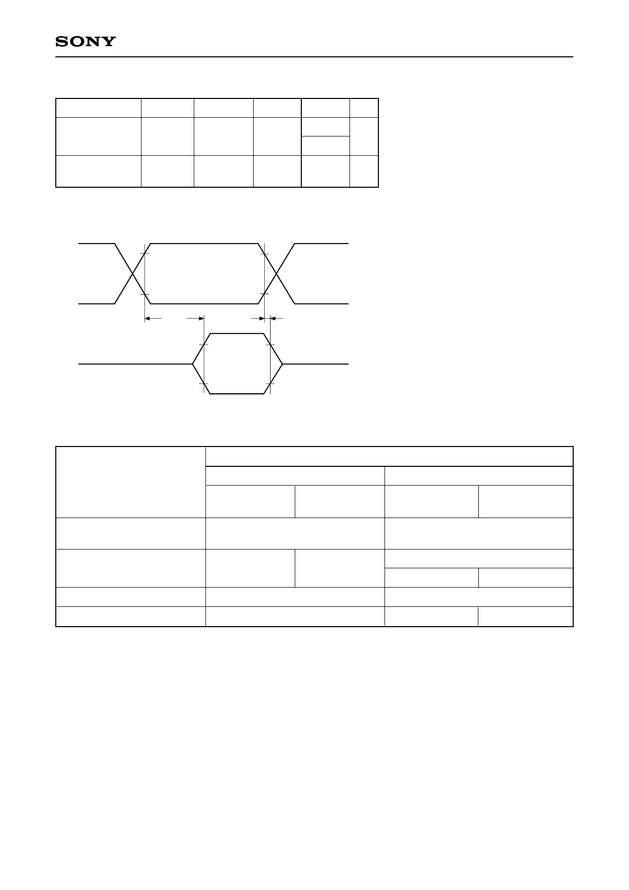
EPROM Read Timing (Ta = –20 to +75°C, VDD = 3.0 to 5.5V, Vss = 0V)
Item
Symbol
Pin
Min.
Address → data
input delay time
tACC
A0 to A15
D0 to D7
Max. Unit
100∗1
75∗2
ns
Address → data
hold time
tIH
A0 to A15
D0 to D7
0
ns
∗1 At 12MHz operation (VDD = 4.5 to 5.5V)
∗2 At 12MHz operation (VDD = 3.0 to 5.5V), At 16MHz operation (VDD = 4.5 to 5.5V)
A0 to A15
D0 to D7
Address data
tACC
Input data
0.8VDD
0.2VDD
tIH
0.8VDD
0.2VDD
CXP81800
Products List
Products
Optional item
Mask product
CXP81840A
CXP81848A
Piggyback/evaluator product
CXP81800-U01Q
CXP81800-U01R
CXP81800-U02R
Package
100-pin plastic QFP/LQFP
100-pin ceramic
PQFP
ROM capacitance
40Kbytes
48Kbytes
EPROM 48Kbytes
27C512 × 1
27C256 × 2
Pull-up resistance for reset pin
Input circuit format∗1
Existent/Non-existent
CMOS schmitt/TTL schmitt
Existent
TTL schmitt
CMOS schmitt
∗1 On PG4 pin and PG5 pin, the input circuit format can be selected to every pin.
–6–
Share Link: 