LC75810E 查看數據表(PDF) - ON Semiconductor
零件编号
产品描述 (功能)
生产厂家
LC75810E Datasheet PDF : 54 Pages
| |||
LC75810E/T
• CGROM (Character generator ROM)
CGROM is the ROM that is used to generate the 240 kinds of 5 × 7, 5 × 8, or 5 × 9 dot matrix character patterns from
the 8-bit character codes. CGROM has a capacity of 240 × 45 bits. When a character code is written to DCRAM, the
character pattern stored in the CGROM corresponding to the character code is displayed at the position on the LCD
corresponding to the DCRAM address loaded into AC.
• CGRAM (Character generator RAM)
CGRAM is the RAM to which user programs can freely write arbitrary character patterns. Up to 16 kinds of 5 × 7, 5 ×
8, or 5 × 9 dot matrix character patterns can be stored. CGRAM has a capacity of 16 × 45 bits.
• ALATCH (Additional data latch)
ALATCH is the latch that is used to store the ADATA display data for the accessory display. ALATCH has a capacity
of 80 bits, and the stored display data is displayed directly without the use of CGROM or CGRAM.
• SC (Scroll counter)
SC is the counter that is used to scroll the display in the left, right, up, or down directions in dot units. Since this
function scrolls in dot units, it implements smooth scrolling.
Reset Function
The LC75810E and LC75810T are reset when a low level is applied to the RES pin at power on and, in normal mode. On a
reset the LC75810E and LC75810T create a display with all LCD panels turned off. However, after a reset applications
must set the contents of DCRAM, ALATCH, and CGRAM before turning on display with a “display on/off control”
instruction since the contents of these memories are undefined. That is, applications must execute the following
instructions.
• Set display technique
• DCRAM data write
• ALATCH data write (If ALATCH is used.)
• CGRAM data write (IF CGRAM is used.)
• Set AC and SC addresses
• Set display contrast (If the display contrast adjustment circuit is used.)
After executing the above instructions, applications must turn on the display with a “display on/off control” instruction.
Note that when applications turn off in the normal mode, applications must turn off the display with a “display on/off
control” instruction. (See the detailed instruction descriptions.)
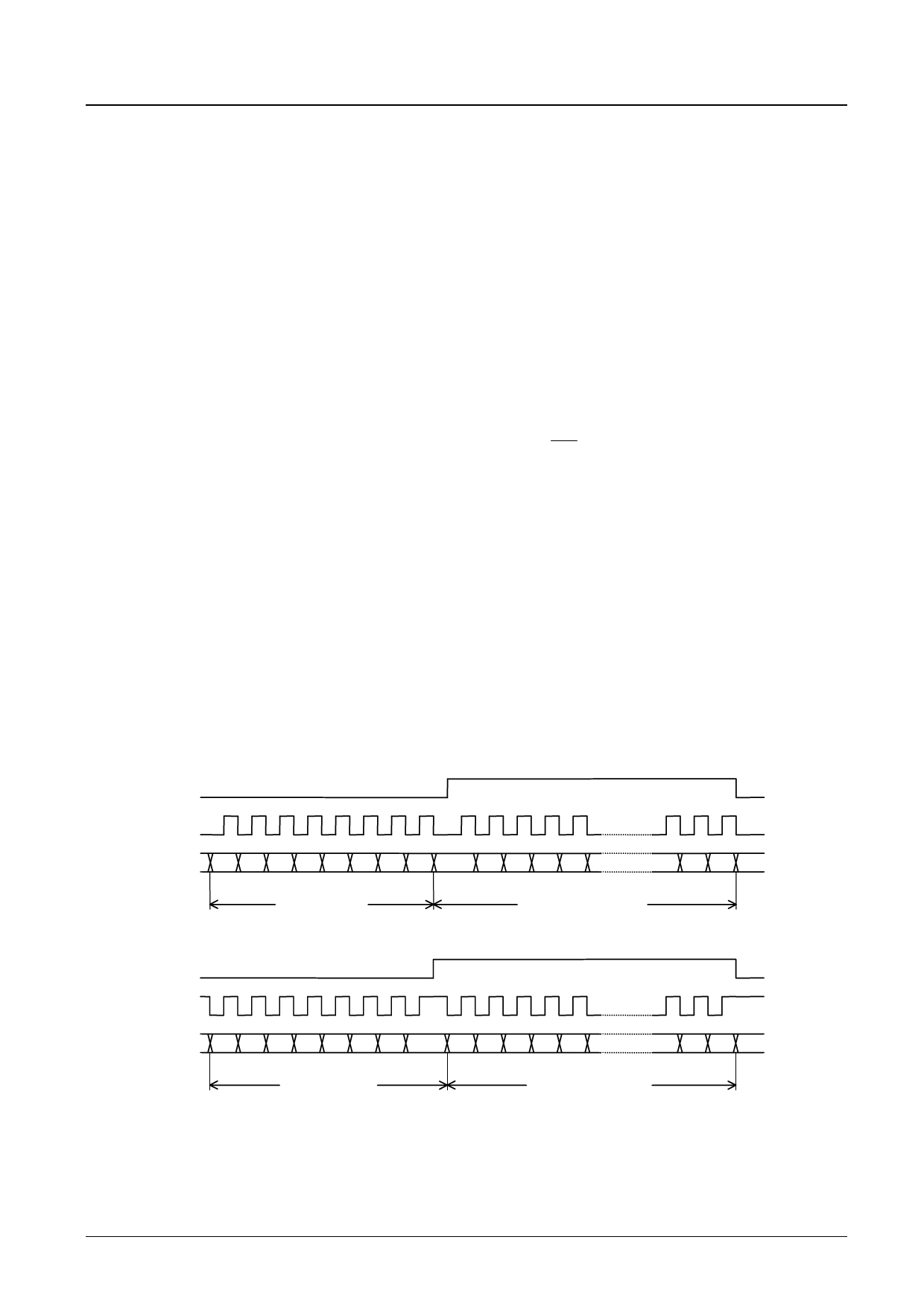
Serial Data Transfer Format
• When CL is stopped at the low level
CE
CL
DI 0 1 1 1 0 0 1 0 D0 D1 D2 D3 D4
B0 B1 B2 B3 A0 A1 A2 A3
CCB address
8 bits
Instruction data
Up to 144 bits
• When CL is stopped at the high level
CE
D142 D143
CL
DI 0 1 1 1 0 0 1 0 D0 D1 D2 D3 D4
B0 B1 B2 B3 A0 A1 A2 A3
D142 D143
CCB address
8 bits
Instruction data
Up to 144 bits
• CCB address: 4EH
• D0 to D143: Instruction data
The data is acquired on the rising edge of the CL signal and latched on the falling edge of the CE signal. When
transferring instruction data from the microcontroller, applications must assure that the time from the transfer of one
set of instruction data until the next instruction data transfer is significantly longer than the instruction execution time.
No.7141-10/54
Share Link: 