LTC1199 查看數據表(PDF) - Linear Technology
零件编号
产品描述 (功能)
生产厂家
LTC1199 Datasheet PDF : 28 Pages
| |||
LTC1197/LTC1197L
LTC1199/LTC1199L
APPLICATIO S I FOR ATIO
Dummy Bit
The dummy bit is a placeholder that extends the acquisi-
tion time of the ADC. This bit can be either high or low and
does not affect the conversion of the ADC.
Operation with DIN and DOUT Tied Together
The LTC1199/LTC1199L can be operated with DIN and
DOUT tied together. This eliminates one of the lines
required to communicate to the microprocessor (MPU).
Data is transmitted in both directions on a single wire. The
processor pin connected to this data line should be
configurable as either an input or an output. The LTC1199/
LTC1199L will take control of the data line and drive it low
on the 4th falling CLK edge after the start bit is received
(see Figure 3). Therefore the processor port line must be
switched to an input before this happens to avoid a
conflict.
In the Typical Applications section, there is an example of
interfacing the LTC1199/LTC1199L with DIN and DOUT
tied together to the Intel 8051 MPU.
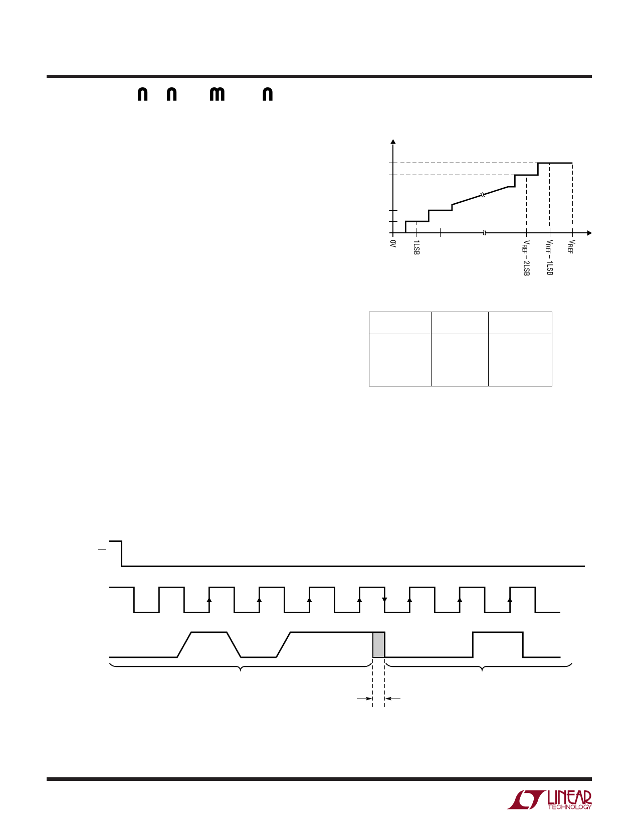
Unipolar Transfer Curve
The LTC1197/LTC1197L/LTC1199/LTC1199L are perma-
nently configured for unipolar only. The input span and
code assignment for this conversion type are shown in the
following figures for a 5V reference.
Unipolar Transfer Curve
1111111111
1111111110
•
•
•
0000000001
VIN
0000000000
1197/99 AI03
Unipolar Output Code
OUTPUT CODE INPUT VOLTAGE
1111111111
1111111110
•
•
0000000001
0000000000
VREF – 1LSB
VREF – 2LSB
•
•
1LSB
0V
INPUT VOLTAGE
(VREF = 5.000V)
4.99512V
4.99023V
•
•
4.88mV
0V
1197/99 AI04
ACHIEVING MICROPOWER PERFORMANCE
With typical operating currents of 5mA (LTC1197/
LTC1199) at 5V and 0.8mA (LTC1197L/LTC1199L) at
2.7V it is possible for these ADCs to achieve true
micropower performance by taking advantage of the
automatic shutdown between conversions. In systems
CS
CLK
DATA (DIN/DOUT)
14
1
2
3
4
START
SGL/DIFF
ODD/SIGN
DUMMY
NULL BITS
B9
B8
MPU CONTROLS DATA LINE AND SENDS
MUX ADDRESS TO LTC1199/LTC1199L
PROCESSOR MUST RELEASE
DATA LINE AFTER 4TH RISING CLK
AND BEFORE THE 4TH FALLING CLK
LTC1199/LTC1199L CONTROL DATA LINE
AND SEND A/D RESULT BACK TO MPU
LTC1199/LTC1199L TAKE CONTROL OF
DATA LINE ON 4TH FALLING CLK
1197/99 F03
Figure 3. LTC1199/LTC1199L Operation with DIN and DOUT Tied Together
Share Link: 