LTC1199 查看數據表(PDF) - Linear Technology
零件编号
产品描述 (功能)
生产厂家
LTC1199 Datasheet PDF : 28 Pages
| |||
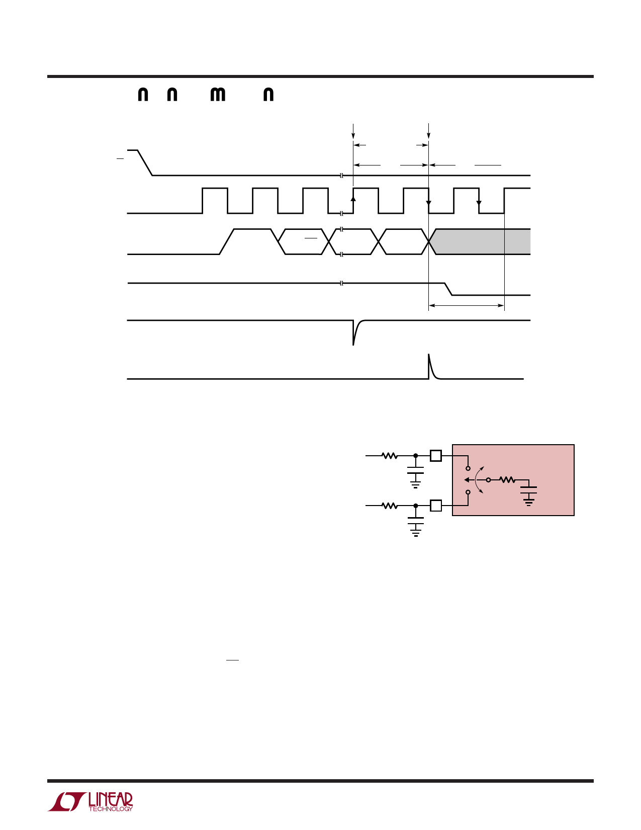
APPLICATIO S I FOR ATIO
CS
CLK
LTC1197/LTC1197L
LTC1199/LTC1199L
SAMPLE
HOLD
“+” INPUT MUST
SETTLE DURING
THIS TIME
tSMPL
tCONV
DIN
START
SGL/DIFF
ODD/SGN
DUMMY
DON‘T CARE
DOUT
“+” INPUT
1ST BIT TEST “–” INPUT MUST
SETTLE DURING THIS TIME
“–” INPUT
Figure 5. LTC1199/LTC1199L “+” and “–” Input Settling Windows
1197/99 F05
ANALOG INPUTS
Because of the capacitive redistribution A/D conversion
techniques used, the analog inputs of the LTC1197/
LTC1197L/LTC1199/LTC1199L have capacitive switching
input current spikes. These current spikes settle quickly
and do not cause a problem if source resistances are less
than 200Ω or high speed op amps are used (e.g., the
LT®1224, LT1191, LT1226 or LT1215). However, if large
source resistances are used or if slow settling op amps
drive the inputs, take care to ensure that the transients
caused by the current spikes settle completely before the
conversion begins.
“+” Input Settling
The input capacitor of the LTC1197/LTC1197L is switched
onto the “+” input in the falling edge of CS and the sample
time continues until the second falling CLK edge (see
Figure 1). However, the input capacitor of the LTC1199/
LTC1199L is switched onto “+” input after ODD/SGN is
clocked into the ADC and remains there until the fourth
falling CLK edge (see Figure 5). The sample time is 1.5 CLK
cycles before conversion starts. The voltage on the “+”
VIN +
RSOURCE +
VIN –
RSOURCE –
“+”
INPUT
C1
“–”
INPUT
C2
LTC1197/LTC1197L
LTC1199/LTC1199L
RON = 200Ω
CIN = 20pF
1197/99 F06
Figure 6. Analog Equivalent Circuit
input must settle completely within tSMPL for the ADC to
perform an accurate conversion. Minimizing RSOURCE+
and C1 will improve the input settling time (see Figure 6).
If a large “+” input source resistance must be used, the
sample time can be increased by using a slower CLK
frequency.
“–” Input Settling
At the end of tSMPL, the input capacitor switches to the
“–” input and conversion starts (see Figures 1 and 5).
During the conversion the “+” input voltage is effectively
“held” by the sample-and-hold and will not affect the
17
Share Link: 