EL5144 查看數據表(PDF) - Renesas Electronics
零件编号
产品描述 (功能)
生产厂家
EL5144 Datasheet PDF : 24 Pages
| |||
EL5144, EL5146, EL5244, EL5246, EL5444
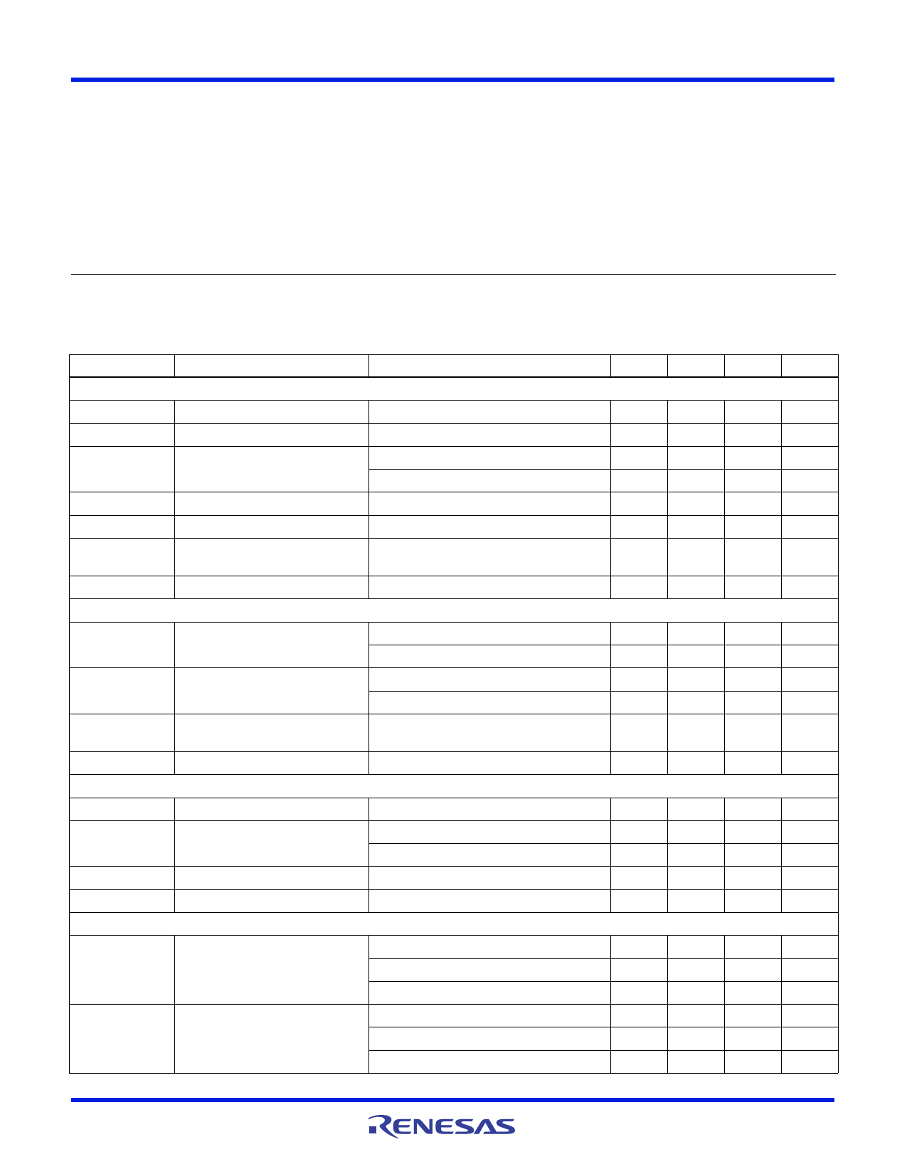
Absolute Maximum Ratings (TA = +25°C)
Supply Voltage between VS and GND. . . . . . . . . . . . . . . . . . . . .+6V
Pin Voltages . . . . . . . . . . . . . . . . . . . . . . . . . GND -0.5V to VS +0.5V
Maximum Continuous Output Current . . . . . . . . . . . . . . . . . . . 50mA
Operating Conditions
Operating Temperature . . . . . . . . . . . . . . . . . . . . . . .-40°C to +85°C
Thermal Information
Power Dissipation . . . . . . . . . . . . . . . . . . . . . . . . . . . . . See Curves
Storage Temperature . . . . . . . . . . . . . . . . . . . . . . . .-65°C to +150°C
Pb-Free Reflow Profile. . . . . . . . . . . . . . . . . . . . . . . . .see link below
http://www.intersil.com/pbfree/Pb-FreeReflow.asp
CAUTION: Do not operate at or near the maximum ratings listed for extended periods of time. Exposure to such conditions may adversely impact product reliability and
result in failures not covered by warranty.
IMPORTANT NOTE: All parameters having Min/Max specifications are guaranteed. Typical values are for information purposes only. Unless otherwise noted, all tests
are at the specified temperature and are pulsed tests, therefore: TJ = TC = TA
Electrical Specifications VS = +5V, GND = 0V, TA = +25°C, CE = +2V, unless otherwise specified.
PARAMETER
DESCRIPTION
CONDITIONS
MIN
TYP
MAX
UNIT
AC PERFORMANCE
dG
Differential Gain Error (Note 1)
G = 2, RL = 150 to 2.5V, RF = 1k
0.1
%
dP
Differential Phase Error (Note 1) G = 2, RL = 150 to 2.5V, RF = 1k
0.1
°
BW
Bandwidth
-3dB, G = 1, RL = 10k RF = 0
100
MHz
-3dB, G = 1, RL = 150 RF = 0
60
MHz
BW1
Bandwidth
±0.1dB, G = 1, RL = 150 to GND, RF = 0
8
MHz
GBWP
Gain Bandwidth Product
60
MHz
SR
Slew Rate
G = 1, RL = 150 to GND, RF = 0, VO = 0.5V 150
200
to 3.5V
V/µs
tS
Settling Time
DC PERFORMANCE
to 0.1%, VOUT = 0V to 3V
35
ns
AVOL
VOS
TCVOS
Open Loop Voltage Gain
RL = no load, VOUT = 0.5V to 3V
54
65
dB
RL = 150 to GND, VOUT = 0.5V to 3V
40
50
dB
Offset Voltage
VCM = 1V, SOT23-5 and MSOP packages
25
mV
VCM = 1V, All other packages
15
mV
Input Offset Voltage Temperature
Coefficient
10
mV/°C
IB
Input Bias Current
INPUT CHARACTERISTICS
VCM = 0V and 3.5V
2
100
nA
CMIR
Common Mode Input Range
CMRR 47dB
0
3.5
V
CMRR
Common Mode Rejection Ratio
RIN
Input Resistance
CIN
Input Capacitance
OUTPUT CHARACTERISTICS
DC, VCM = 0 to 3.0V
DC, VCM = 0 to 3.5V
50
60
dB
47
60
dB
1.5
G
1.5
pF
VOP
VON
Positive Output Voltage Swing
Negative Output Voltage Swing
RL = 150 to 2.5V (Note 2)
RL = 150 to GND (Note 2)
RL = 1k to 2.5V (Note 2)
RL = 150 to 2.5V (Note 2)
RL = 150 to GND (Note 2)
RL = 1k to 2.5V (Note 2)
4.70
4.85
V
4.20
4.65
V
4.95
4.97
V
0.15
0.30
V
0
V
0.03
0.05
V
FN7177 Rev 2.00
March 31, 2011
Page 5 of 24
Share Link: 