AN-6073 查看數據表(PDF) - Fairchild Semiconductor
零件编号
产品描述 (功能)
生产厂家
AN-6073 Datasheet PDF : 13 Pages
| |||
AN-6073
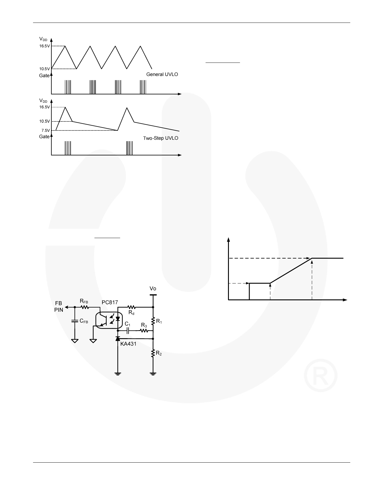
Figure 8. UVLO Effect
FB Input
The FAN6751 is designed for peak-current-mode control. A
current-to-voltage conversion is done externally with a
current-sense resistor RS. Under normal operation, the FB
level controls the peak inductor current:
VSENSE
= Ipk
× RS
= VFB − 0.6
4
(2)
where VFB is the voltage on FB pin and 4 is an internal
divider ratio.
When VFB is less than 0.6V, the FAN6751 terminates the
output pulses.
APPLICATION NOTE
down at no load. The value of the biasing resistor Rb is
determined as:
Vo −VD −VZ • K ≥ 1.5mA
Rb
(3)
where:
VD is the drop voltage of photodiode, approximately 1.2V;
VZ is the minimum operating voltage, 2.5V of the shunt
regulator; and
K is the current transfer rate (CTR) of the opto-coupler.
For an output voltage VO=5V with CTR=100%, the
maximum value of Rb is 860Ω.
Green Mode Operation
Green mode includes off-time modulation and burst mode to
reduce the PWM frequency at light-load and in no-load
conditions. The feedback voltage of the FB pin is taken as a
reference. When the feedback voltage is lower than VFB-N,
the PWM frequency decreases. Because most losses in a
switching-mode power supply are proportional to the PWM
frequency, the off-time modulation reduces the power
consumption of the power supply at light-load and no-load
conditions. Figure 10 is the PWM frequency is 65KHz at
nominal load and decreases to 18KHz at light load.
Frequency
Fosc:65KHz
PWM Frequency
Fosc:18KHz
VFB-ZDC
VFB-G
VFB-N
Figure 10. PWM Frequency vs. FB Voltage
Figure 9. Feedback Circuit
Figure 9 is a typical feedback circuit consisting mainly of a
shunt regulator and an opto-coupler. R1 and R2 form a
voltage divider for the output voltage regulation. R3 and C1
are adjusted for control-loop compensation. A small-value
RC filter (e.g. RFB= 100Ω, CFB= 1nF) placed on the FB pin
to the GND can further increase the stability. The maximum
sourcing current of the FB pin is 1.5mA. The phototransistor
must be capable of sinking this current to pull FB level
The power supply enters “burst mode” in no-load
conditions. As shown in Figure 11 and Figure 12, when VFB
drops below VFB-ZDC, the PWM output is shuts off and the
output voltage drops at a rate dependent on load current.
This causes the feedback voltage to rise. Once VFB exceeds
VFB-ZDC, the internal circuit starts to provide switching pulse.
The feedback voltage then falls and the process repeats.
Burst mode operation alternately enables and disables
switching of the MOSFET, reducing the switching losses in
standby mode.
© 2008 Fairchild Semiconductor Corporation
Rev. 1.0.0 • 9/26/08
4
www.fairchildsemi.com
Share Link: 