AN-6073 查看數據表(PDF) - Fairchild Semiconductor
零件编号
产品描述 (功能)
生产厂家
AN-6073 Datasheet PDF : 13 Pages
| |||
AN-6073
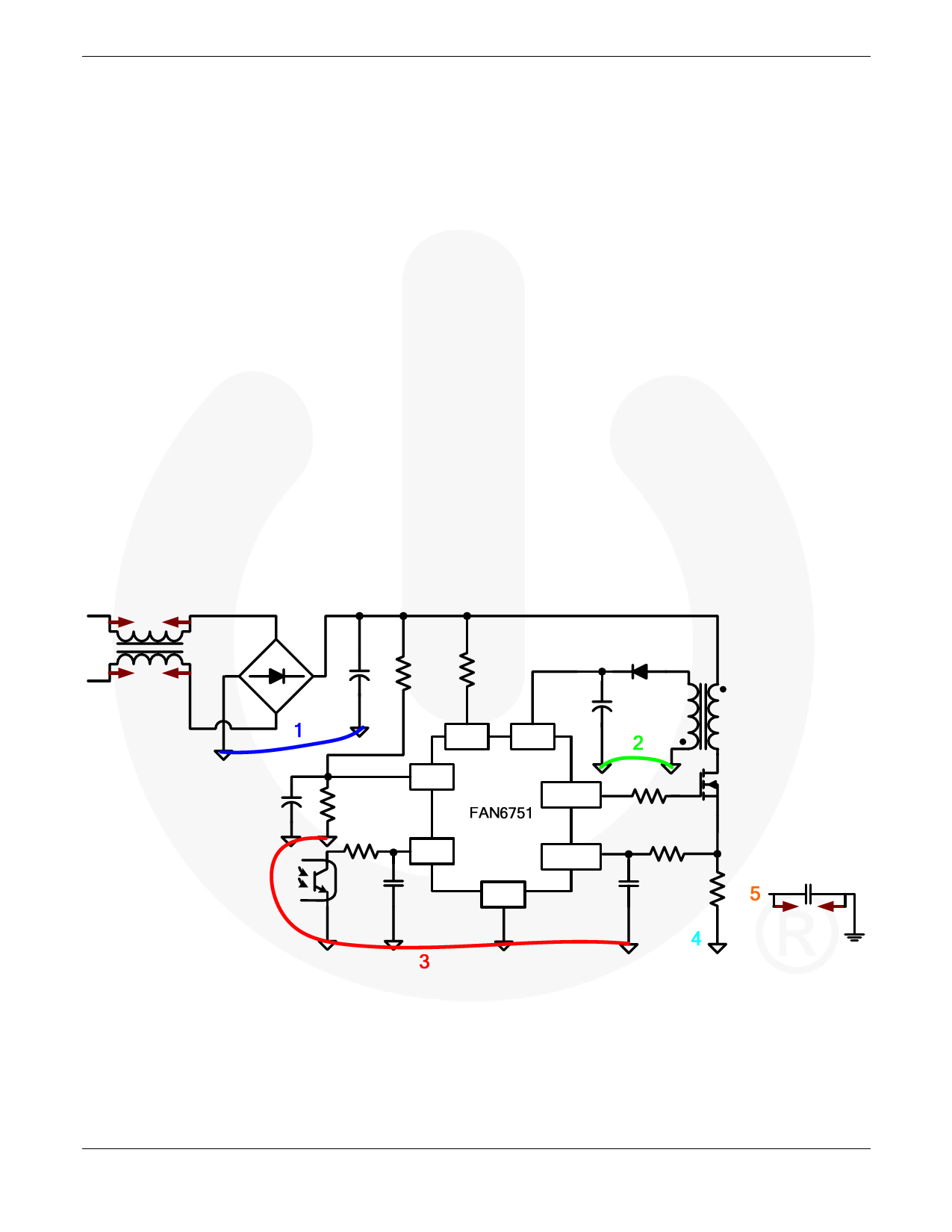
Printed Circuit Board Layout
Current/voltage/switching frequency makes printed circuit
board layout and design a very important issue. Good PCB
layout minimizes excessive EMI and prevents the power
supply from being disrupted during surge/ESD tests. The
following are some general guidelines:
To get better EMI performance and reduce line frequency
ripples, the output of the bridge rectifier should be
connected to capacitor Cbulk first, then to the switching
circuits.
The high-frequency current loop is found in Cbulk –
Transformer – MOSFET – RS – Cbulk. The area
enclosed by this current loop should be as small as
possible. Keep the traces (especially 4→1) short, direct,
and wide. High-voltage drain traces related to the
MOSFET and RCD snubber should be kept far way from
control circuits to prevent unnecessary interference. If a
heatsink is used for the MOSFET, it is recommended to
ground the heatsink.
As indicated by 3, the control circuit’s ground should be
connected first, then to other circuitry.
As indicated by 2, the area enclosed by the transformer
auxiliary winding, D1, and C1, should be kept small.
Place C1 close to the FAN6751 for good decoupling.
APPLICATION NOTE
Two suggestions with different pros and cons for ground
connections are recommended.
GND3→2→4→1: Possible method for circumventing the
sense signals common impedance interference.
GND3→2→1→4: Potentially better for ESD testing
where a ground is not available for the power supply. The
charges for ESD discharge path go from the secondary
through the transformer stray capacitance to the GND2
first. Then, the charges go from GND2 to GND1 and
back to the mains. Control circuits should not be placed
on the discharge path. Point discharge for common choke
can decrease high-frequency impedance and help increase
ESD immunity.
Should a Y-cap between primary and secondary be
required, the Y-cap should be connected to the positive
terminal of the Cbulk (VDC). If this Y-cap is connected to
the primary GND, it should be connected to the negative
terminal of the Cbulk (GND1) directly. Point discharge of
the Y-cap also helps with ESD. However, according to
safety requirements, the creepage between the two
pointed ends should be at least 5mm.
Common
mode
choke
BD1
CBulk
R1
RHV
HV VDD
D1
CVDD
VIN
C2
R2
Rg
GATE
FB
RFB
CFB
SENSE
GND
RLF
CLF
CFB
RS
Figure 22. Layout Considerations
© 2008 Fairchild Semiconductor Corporation
Rev. 1.0.0 • 9/26/08
9
www.fairchildsemi.com
Share Link: 