MC78LC33NTR 查看數據表(PDF) - Motorola => Freescale
零件编号
产品描述 (功能)
生产厂家
MC78LC33NTR Datasheet PDF : 8 Pages
| |||
MC78LC00 Series
APPLICATIONS INFORMATION
Introduction
The MC78LC00 micropower voltage regulators are
specifically designed with high accuracy output voltage and
ultra low quiescent current by CMOS process making them
ideal for battery powered applications and hand–held
communication equipment. An input bypass capacitor is
recommended if the regulator is located an appreciable
distance (≥ 4 inches) from the input voltage source. These
regulators require ≥ 0.1 µF capacitance between the output
terminal and ground for stability. Most types of aluminum,
tantalum or multilayer ceramic will perform adequately. Solid
tantalums or other appropriate capacitors are recommended
for operation below 25°C. The bypass capacitors should be
mounted with the shortest possible leads or track lengths
directly across the regulator input and output terminals.
With economical electrolytic capacitors, cold temperature
operation can pose a serious stability problem. As the
electrolyte freezes, around –30°C, the capacitance will
decrease and the equivalent series resistance (ESR) will
increase drastically, causing the circuit to oscillate. Quality
electrolytic capacitors with extended temperature ranges of
–40° to +85°C are readily available. Solid tantalum
capacitors may be the better choice if small size is a
requirement. However, a maximum ESR limit of 3.0 Ω must
be observed over temperature to maintain stability.
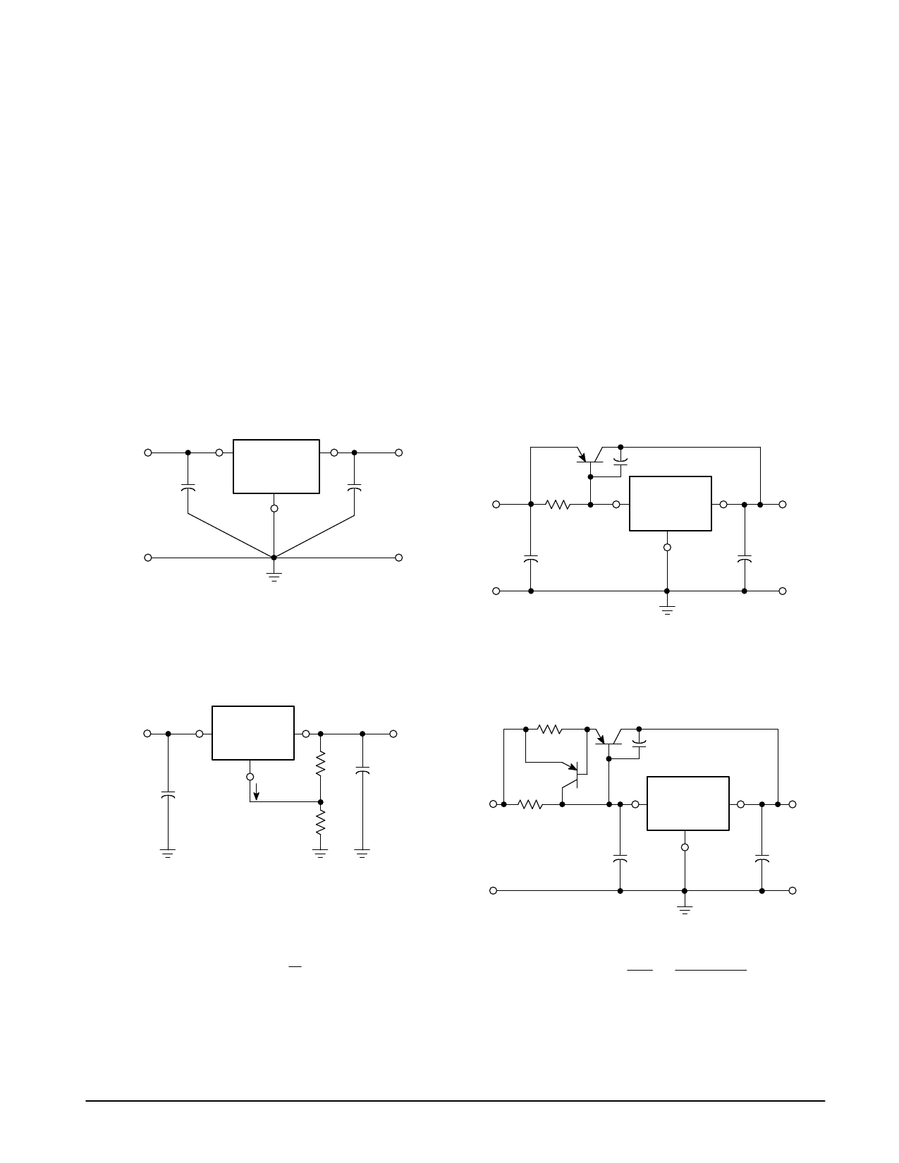
In the Current Boost Circuit, shown in Figures 10 and 12,
an output current of up to 600 mA can be delivered by the
circuit. The circuit of Figure 10 has no current limit. In each
case, the external transistor must be rated for the expected
power dissipation. Figure 11 shows how a fixed output may
be programmed, using R1 and R2, to provide a higher
output voltage.
Figure 9. Typical Application
Vin
0.1 µF
2
3
MC78LC00
1
VO
0.1 µF
Gnd
Gnd
Figure 10. Current Boost Circuit
MJD32C
.033 µF
100
2
3
Vin
MC78LC00
VO
0.1 µF
Gnd
1
0.1 µF
Gnd
Vin
C1
Figure 11. Adjustable VO
2
3
MC78LC00
R1
1
ICC
Gnd
R2
VO
C2
ǒ Ǔ + ) ) VO
VO(Reg) 1
R2
R1
ICC R2
Figure 12. Current Boost Circuit with
Overcurrent Limit Circuit
R2 MJD32C
Q1
Q2
.033 µF
MMBT2907
ALT1
Vin
R1
0.1 µF
Gnd
2
3
MC78LC00
1
VO
0.1 µF
Gnd
[ ) ) IO(short circuit)
VBE2
R2
VBE1 VBE2
R1
MOTOROLA ANALOG IC DEVICE DATA
5
Share Link: 