FDC6331L 查看數據表(PDF) - Fairchild Semiconductor
零件编号
产品描述 (功能)
生产厂家
FDC6331L Datasheet PDF : 4 Pages
| |||
Electrical Characteristics
Symbol
Parameter
Off Characteristics
BV IN
Vin Breakdown Voltage
ILoad
Zero Gate Voltage Drain Current
IFL
Leakage Current, Forward
IRL
Leakage Current, Reverse
On Characteristics (Note 2)
VON/OFF (th) Gate Threshold Voltage
RDS(on)
Static Drain–Source
On–Resistance (Q2)
RDS(on)
Static Drain–Source
On–Resistance (Q1)
TA = 25°C unless otherwise noted
Test Conditions
VON/OFF = 0 V, ID = –250 PA
VIN = 6.4 V, VON/OFF = 0 V
VON/OFF = 0 V, VIN = 8 V
VON/OFF = 0 V, VIN = –8 V
VIN = VON/OFF, ID = –250 PA
VGS = –4.5 V,
VGS = –2.5 V,
VGS = –1.8 V,
ID = –2.8A
ID = –2.5 A
ID = –2.0 A
VGS = 4.5 V,
VGS = 2.7 V,
ID = 0.4A
ID = 0.2 A
Min Typ Max Units
8
V
–1
PA
–100 nA
100 nA
0.4 0.9
34
45
64
3.1
3.8
1.5
V
55 m:
70
100
4
:
5
Drain–Source Diode Characteristics and Maximum Ratings
IS
Maximum Continuous Drain–Source Diode Forward Current
VSD
Drain–Source Diode Forward
Voltage
VON/OFF = 0 V, IS = –0.6 A (Note 2)
–0.6 A
–1.2 V
Notes:
1. R TJA is the sum of the junction-to-case and case-to-ambient thermal resistance where the case thermal reference is defined as the solder mounting
surface of the drain pins. R TJC is guar anteed by design while R TJA is determined by the user’s board design.
2. Pulse Test: Pulse Width < 300μs, Duty Cycle < 2.0%.
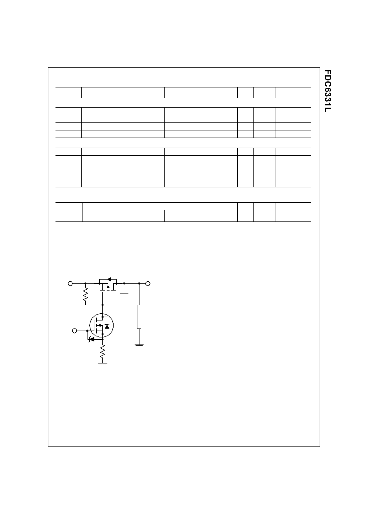
FDC6331L Load Switch Application Circuit
IN
Q2
OUT
C1
R1
Q1
ON/OFF
LOAD
R2
External Component Recommendation:
For additional in-rush current control, R2 and C1 can be added. For more information, see application note AN1030.
FDC6331L Rev D
Share Link: 