HI5741BIB-T 查看數據表(PDF) - Renesas Electronics
零件编号
产品描述 (功能)
生产厂家
HI5741BIB-T Datasheet PDF : 13 Pages
| |||
HI5741
Detailed Description
The HI5741 is a 14-bit, current out D/A converter. The DAC
can convert at 100 MSPS and runs on +5V and -5.2V supplies.
The architecture is an R/2R and segmented switching current
cell arrangement to reduce glitch. Laser trimming is employed
to tune linearity to true 14-bit levels. The HI5741 achieves its
low power and high speed performance from an advanced
BiCMOS process. The HI5741 consumes 650mW (typical) and
has an improved hold time of only 0.25ns (typical). The HI5741
is an excellent converter for use in communications
applications and high performance video systems.
Digital Inputs
The HI5741 is a TTL/CMOS compatible D/A. Data is latched by
a Master register. Once latched, data inputs D0 (LSB) through
D13 (MSB) are internally translated from TTL to ECL. The
internal latch and switching current source controls are
implemented in ECL technology to maintain high switching
speeds and low noise characteristics.
Decoder/Driver
The architecture employs a split R/2R ladder and segmented
current source arrangement. Bits D0 (LSB) through D9 directly
drive a typical R/2R network to create the binary weighted current
sources. Bits D10 through D13 (MSB) pass through a
“thermometer” decoder that converts the incoming data into 15
individual segmented current source enables. This split
architecture helps to improve glitch, thus resulting in a
more constant glitch characteristic across the entire output
transfer function.
Clocks and Termination
The internal 14-bit register is updated on the rising edge of the
clock. Since the HI5741 clock rate can run to 100 MSPS, to
minimize reflections and clock noise into the part, proper
termination should be used. In PCB layout clock runs should be
kept short and have a minimum of loads. To guarantee
consistent results from board to board, controlled impedance
PCBs should be used with a characteristic line impedance ZO of
50.
To terminate the clock line, a shunt terminator to ground is the
most effective type at a 100 MSPS clock rate. A typical value
for termination can be determined by the equation:
RT = ZO
for the termination resistor. For a controlled impedance board
with a ZO of 50, the RT = 50. Shunt termination is best used
at the receiving end of the transmission line or as close to the
HI5741 CLK pin as possible.
ZO = 50
CLK
RT = 50
HI5741
DAC
FIGURE 20. HI5741 CLOCK LINE TERMINATION
Rise and Fall times and propagation delay of the line will be
affected by the shunt terminator. The terminator should be
connected to DGND.
Noise Reduction
To reduce power supply noise, separate analog and digital
power supplies should be used with 0.1F and 0.01F ceramic
capacitors placed as close to the body of the HI5741 as
possible on the analog (AVEE) and digital (DVEE) supplies.
The analog and digital ground returns should be connected
together back at the device to ensure proper operation on
power up. The VCC power pin should also be decoupled with a
0.1F capacitor.
Reduction of digital noise (caused by high slew rates on the bit
inputs to the HI5741) can be accomplished through the use of
series termination resistors. The use of serial resistors, which
combine with the input capacitance of the HI5741 to induce a low
pass filter characteristic, keeps the noise generated by high slew
rate digital signals from corrupting the high accuracy analog data.
Refer to Application Note AN9619 “Optimizing setup conditions
for high accuracy measurements of the HI5741” for further details
on selecting the proper value of series termination to meet
application specific needs.
Reference
The internal reference of the HI5741 is a -1.23V (typical)
bandgap voltage reference with 50V/°C of temperature drift
(typical). The internal reference is connected to the Control
Amplifier which in turn drives the segmented current cells.
Reference Out (REF OUT) is internally connected to the Control
Amplifier. The Control Amplifier Output (CTRL OUT) should be
used to drive the Control Amplifier Input (CTRL IN) and a 0.1F
capacitor to analog VEE. This improves settling time by
providing an AC ground at the current source base node. The
Full Scale Output Current is controlled by the REF OUT pin and
the set resistor (RSET). The ratio is:
IOUT (Full Scale) = (VREF OUT/RSET) x 16.
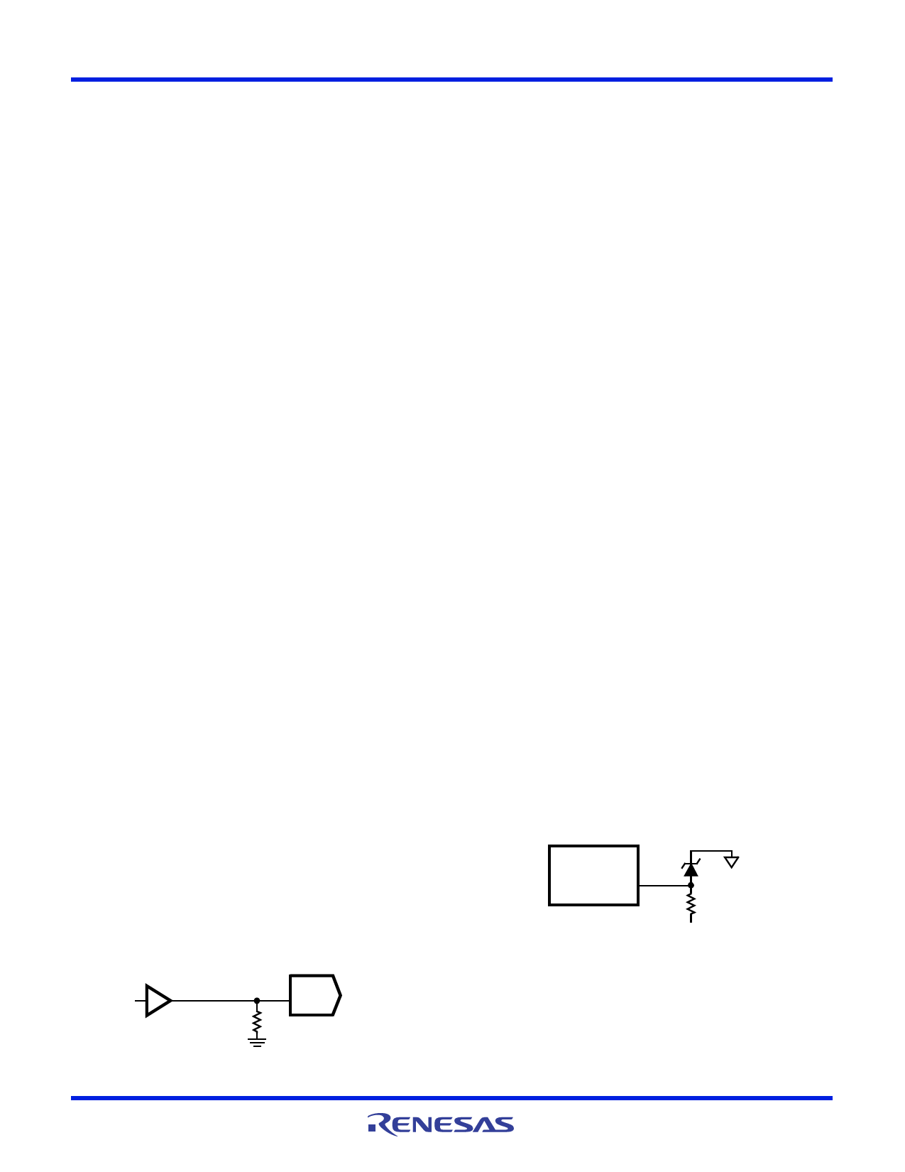
The internal reference (REF OUT) can be overdriven with a
more precise external reference to provide better performance
over temperature. Figure 21 illustrates a typical external
reference configuration.
HI5741
(26) REF OUT
-1.25V
R
-5.2V
FIGURE 21. EXTERNAL REFERENCE CONFIGURATION
Multiplying Capability
The HI5741 can operate in two different multiplying
configurations. For frequencies from DC to 100kHz, a signal of
up to 0.6VP-P can be applied directly to the REF OUT pin as
shown in Figure 22.
FN4071 Rev 12.00
September 20, 2006
Page 9 of 13
Share Link: 