CXP5078 查看數據表(PDF) - Sony Semiconductor
零件编号
产品描述 (功能)
生产厂家
CXP5078 Datasheet PDF : 18 Pages
| |||
CXP5076/5078
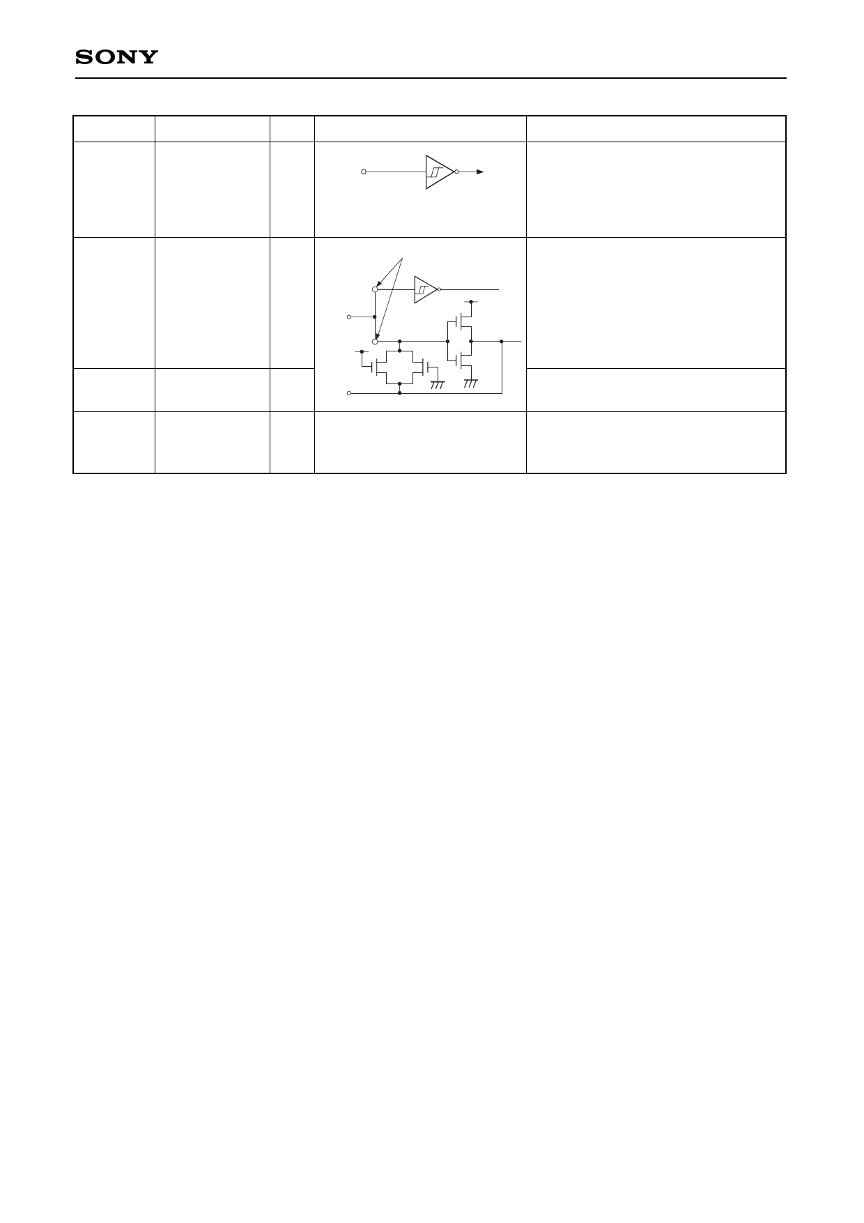
Symbol
Name
I/O
Equivalent Circuit
Description
WP
Wake-up
input
I
Schmitt inverter input
It is the input pin to release the
standby mode, and release by "1".
TEX
TX
VREF
32kHz T/C
clock input
I
TEX
32kHz T/C
clock output
Reference
voltage input
O
TX
I
Mask option
P
N
NP
Input pin for 32kHz timer clock
generation circuit. Connect the
32.768kHz crystal oscillator between
TEX and TX. When using as the
event clock input, connect the clock
oscillation source to the TEX pin,
open the TX pin.
Output of clock generation circuit
Reference voltage input for power
supply voltage resetting circuit.
Connect the zener diode normally.
For all output ports, the output states of ports during standby possible to be programmed to the state holding
before standby or the change to the high impedance.
When the pull-up resistor output is selected, it becomes a pulled-up state even it is input port.
During standby, it is impossible to change to the high impedance of PY0 and PY1 in the inverter output state. To
change to the high impedance, select the pull-up resistor output, and then set to the high level output ("1" state).
–7–
Share Link: 