LCX007CL 查看數據表(PDF) - Sony Semiconductor
零件编号
产品描述 (功能)
生产厂家
LCX007CL Datasheet PDF : 24 Pages
| |||
LCX007CL
Absolute Maximum Ratings (VSS = 0V)
• H driver supply voltage
HVDD
–1.0 to +20 V
• V driver supply voltage
VVDD
–1.0 to +20 V
• Common pad voltage
COM
–1.0 to +17 V
• H shift register input pin voltage HST, HCK1, HCK2
–1.0 to +17 V
RGT, WID
• V shift register input pin voltage VST, VCK, PCG
–1.0 to +17 V
CLR, ENB, DWN
• Video signal input pin voltage
SIG1, SIG2, SIG3, SID –1.0 to +15 V
• Operating temperature
Topr
–10 to +70 °C
• Storage temperature
Tstg
–30 to +85 °C
Operating Conditions (VSS = 0V)
• Supply voltage
HVDD
15.7
+0.3
–0.4
V
VVDD
15.7
+0.3
–0.4
V
• Input pulse voltage (Vp-p of all input pins except video signal and side black signal input pins)
Vin
5.0 ± 0.5 V
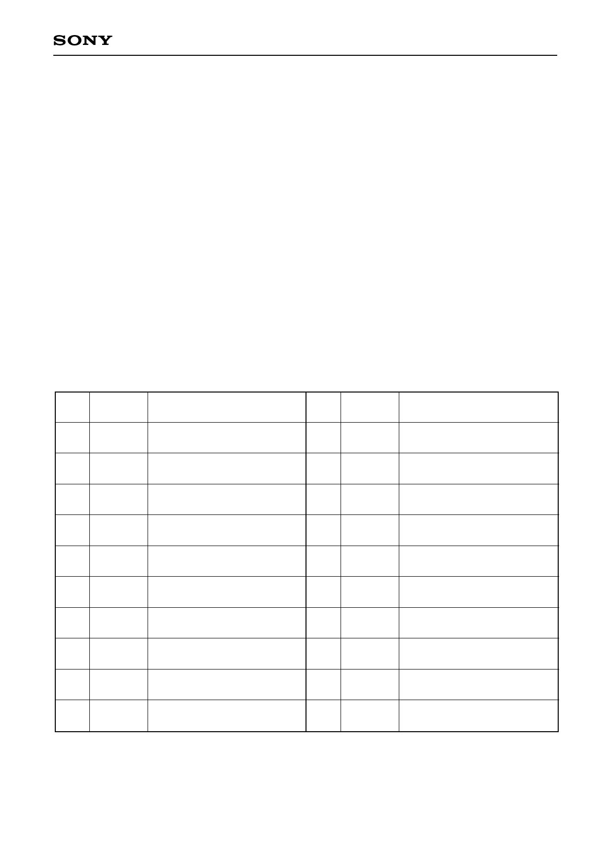
Pin Description
Pin
No.
Symbol
Description
1 SID
Side black signal for 4:3 display
2 SIG1 (G) Video signal (G∗1) to panel
3 SIG2 (R) Video signal (R∗1) to panel
Pin
No.
Symbol
11 HCK2
12 CLR
Description
Clock pulse for H shift register
drive
Improvement pulse (1) for
uniformity
13 ENB
Enable pulse for gate selection
4 SIG3 (B) Video signal (B∗1) to panel
5 HVDD
6 WID
7 RGT
8 HST
Power supply for H driver
Aspect-ratio switching
(H: 16:9, L: 4:3)
Drive direction pulse for H shift
register (H: normal, L: reverse)
Start pulse for H shift register
drive
14 VCK
15 PCG
16 VST
17 DWN
18 VVDD
Clock pulse for V shift register
drive
Improvement pulse (2) for
uniformity
Start pulse for V shift register
drive
Drive direction pulse for V shift
register (H: normal, L: reverse)
Power supply for V driver
9 Vss
GND (H, V drivers)
19 COM
Common voltage of panel
10 HCK1
Clock pulse for H shift register
drive
20 TEST
Test; Open
∗1 (R), (G) and (B) are indicated for convenience to show the correspondence with the dot arrangement
diagram.
–3–
Share Link: 