CXD2436Q 查看數據表(PDF) - Sony Semiconductor
零件编号
产品描述 (功能)
生产厂家
CXD2436Q Datasheet PDF : 34 Pages
| |||
CXD2436Q
Description of Operation
• Sync input pins
The CXD2436Q has three types of sync input pins.
Pin No. Symbol SLSY setting
Application
1 HD1IN
2 VD1IN
—
SYNC input pins for VGA
5 CSYNC
H
CSYNC input pin for NTSC/PAL
16 HD2IN
17 VD2IN
L
Separate SYNC input pins for NTSC/PAL
• Clock input pins
The CXD2436Q has two clock input pin systems to support two types of PLL circuits.
1) When using EXT-CKI (using an external PLL IC)
The 1/N frequency divider output is output from the HDN and XHDN pins for the external PLL IC.
The used pins are shown in the following table. (SLCKI = Low)
Pin No. Symbol
30 EXT-CKI
68 HDN
69 XHDN
Application
Clock input
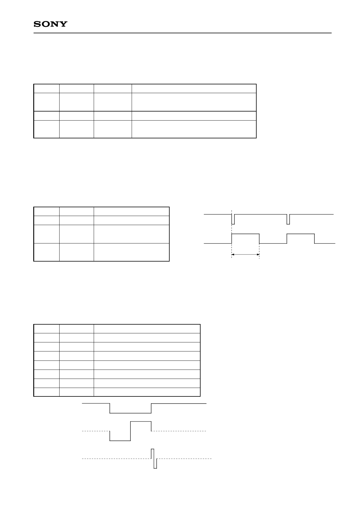
HSYNC
Phase comparison output
(positive polarity)
HDN OUTPUT
Phase comparison output
(negative polarity)
400 clk
2) When using CKI
This system uses the built-in phase comparator and an externally attached VCO circuit (see the Application
Circuit).
This system is used during AV mode (NTSC/PAL).
The used pins are shown in the following table. (Effective when SLCKI is set to High.)
Pin No.
31
32
33
34
35
38
39
Symbol
PEO
PWM
CKO
CKI
RPD
FPD
TC
HSYNC
Application
Loop filter integrator output
Loop filter integrator input
Clock output (oscillation cell output)
Clock input (oscillation cell input)
Phase comparator output
Phase comparator output
FPD pin pulse width adjustment
RPD
An outline of the output waveforms during
PLL lock is shown in the figure to the left.
FPD
—9—
Share Link: 