TISP2072F3DR 查看數據表(PDF) - Power Innovations
零件编号
产品描述 (功能)
生产厂家
TISP2072F3DR Datasheet PDF : 17 Pages
| |||
TISP2072F3, TISP2082F3
DUAL SYMMETRICAL TRANSIENT
VOLTAGE SUPPRESSORS
MARCH 1994 - REVISED SEPTEMBER 1997
APPLICATIONS INFORMATION
protection voltage
The protection voltage, (V(BO) ), increases under lightning surge conditions due to thyristor regeneration. This
increase is dependent on the rate of current rise, di/dt, when the TISP is clamping the voltage in its
breakdown region. The V(BO) value under surge conditions can be estimated by multiplying the 50 Hz rate
V(BO) (250 V/ms) value by the normalised increase at the surge’s di/dt (Figure 7.) . An estimate of the di/dt
can be made from the surge generator voltage rate of rise, dv/dt, and the circuit resistance.
As an example, the CCITT IX K17 1.5 kV, 10/700 µs surge has an average dv/dt of 150 V/µs, but, as the rise
is exponential, the initial dv/dt is higher, being in the region of 450 V/µs. The instantaneous generator output
resistance is 25 Ω. If the equipment has an additional series resistance of 20 Ω, the total series resistance
becomes 45 Ω. The maximum di/dt then can be estimated as 450/45 = 10 A/µs. In practice the
measured di/dt and protection voltage increase will be lower due to inductive effects and the finite slope
resistance of the TISP breakdown region.
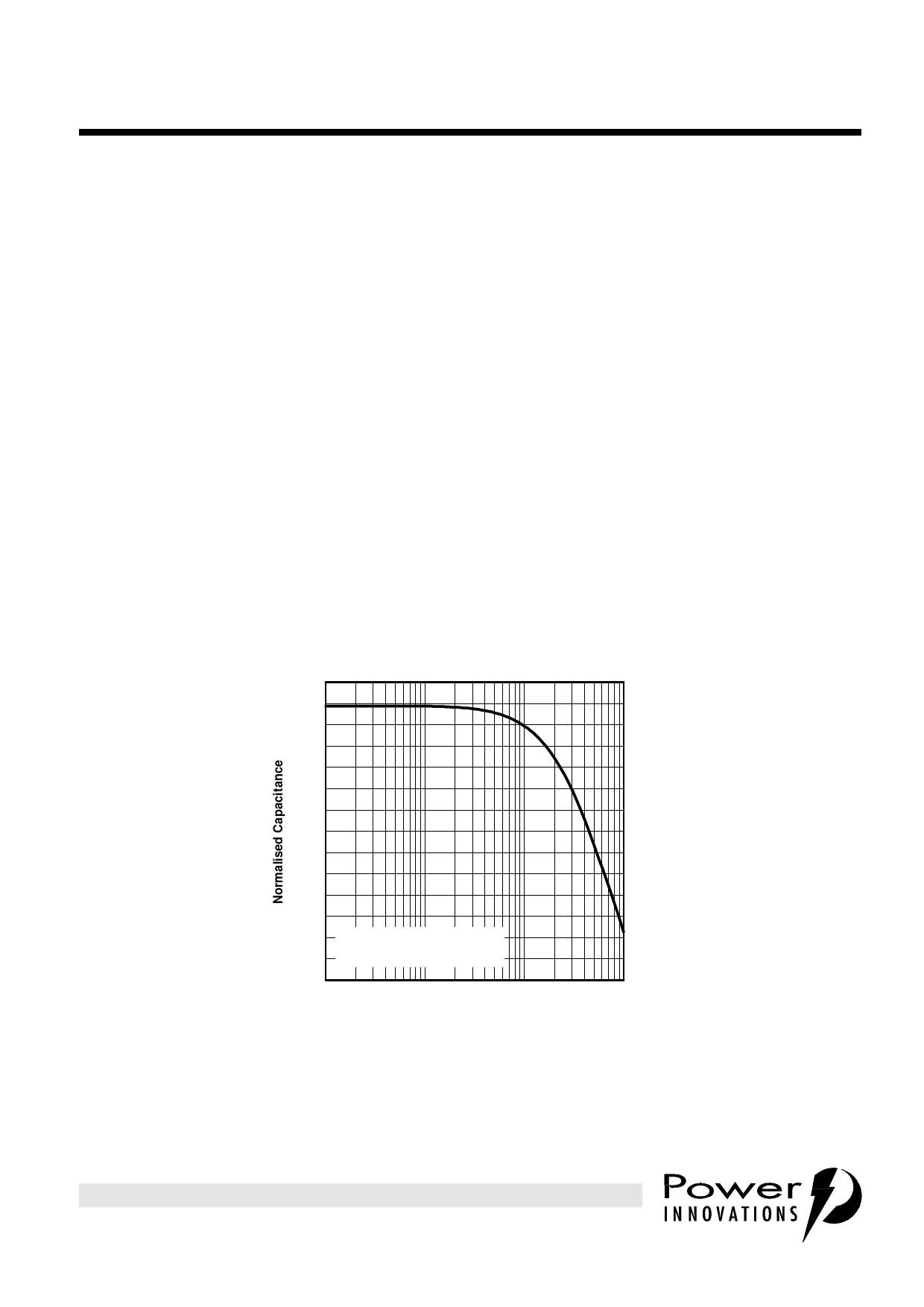
capacitance
off-state capacitance
The off-state capacitance of a TISP is sensitive to junction temperature, TJ , and the bias voltage, comprising
of the dc voltage, VD , and the ac voltage, Vd . All the capacitance values in this data sheet are measured
with an ac voltage of 100 mV. The typical 25°C variation of capacitance value with ac bias is shown in Figure
21. When VD >> Vd the capacitance value is independent on the value of Vd . The capacitance is essentially
constant over the range of normal telecommunication frequencies.
NORMALISED CAPACITANCE
vs
RMS AC TEST VOLTAGE
AIXXAA
1.05
1.00
0.95
0.90
0.85
0.80
0.75
Normalised to Vd = 100 mV
DC Bias, VD = 0
0.70
1
10
100
Vd - RMS AC Test Voltage - mV
Figure 21.
1000
PRODUCT INFORMATION
11
Share Link: 