MAX4305EUK-T 查看數據表(PDF) - Maxim Integrated
零件编号
产品描述 (功能)
生产厂家
MAX4305EUK-T Datasheet PDF : 12 Pages
| |||
740MHz, Low-Noise, Low-Distortion
Op Amps in SOT23-5
RG
RF
RG
RF
FB
IB-
IB+
IN
RS
OUT
VOUT
MAX4104
MAX4105
MAX4304
MAX4305
IN-
75Ω CABLE
IN+
RT
75Ω
RT
OUT 75Ω
75Ω CABLE
RL
MAX4104
75Ω
MAX4105
MAX4304
MAX4305
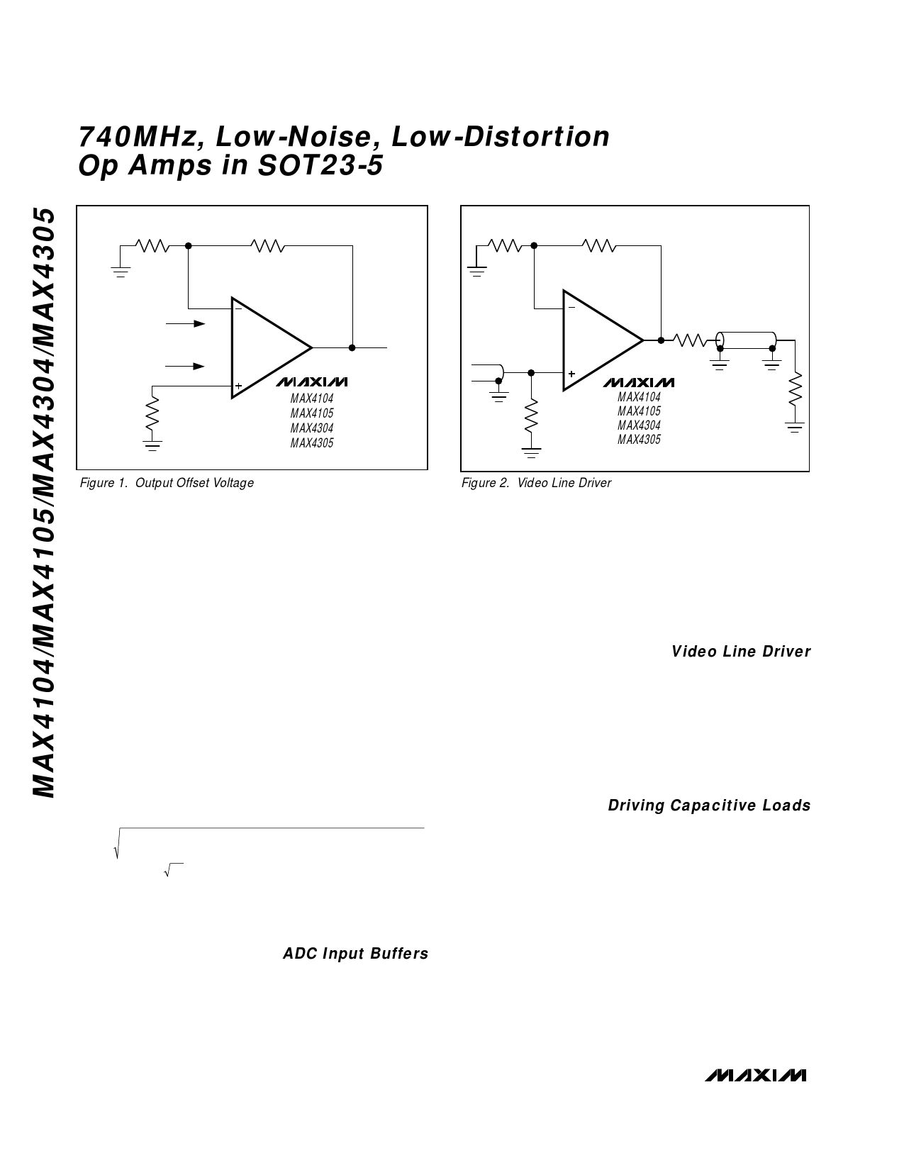
Figure 1. Output Offset Voltage
where:
in = input current noise density (in pA/√Hz)
en = input voltage noise density (in nV/√Hz)
The MAX4104/MAX4105/MAX4304/MAX4305 have a
very low, 2.1nV/√Hz input voltage noise density and
3.1pA/√Hz input current noise density.
An example of DC-error calculations, using the
MAX4304 typical data and the typical operating circuit
with RF = RG = 330Ω (RF || RG = 165Ω) and RS = 50Ω
gives:
( ) ( ) [ ] VOUT
=
32
x
10−6
50
+
32
x
10 −6
165Ω
+1
x
10 −3
1
+
1
VOUT = 15.8mV
Calculating total output noise in a similar manner yields
the following:
en(OUT) =
[ ] 1+1
3. 1
x
10−12
x
50 2 +
3.1
x
10−12
x
165 2
+
2.1
x
10−9
2
en(OUT) = 4.3nV Hz
With a 200MHz system bandwidth, this calculates to
60.8µVRMS (approximately 365µVp-p, using the six-
sigma calculation).
ADC Input Buffers
Input buffer amplifiers can be a source of significant
error in high-speed ADC applications. The input buffer
is usually required to rapidly charge and discharge the
ADC’s input, which is often capacitive. In addition, the
input impedance of a high-speed ADC often changes
Figure 2. Video Line Driver
very rapidly during the conversion cycle—a condition
that demands an amplifier with very low output imped-
ance at high frequencies to maintain measurement
accuracy. The combination of high-speed, fast slew
rate, low noise, and low-distortion available in the
MAX4104/MAX4105/MAX4304/MAX4305 makes them
ideally suited for use as buffer amplifiers in high-speed
ADC applications.
Video Line Driver
The MAX4104/MAX4105/MAX4304/MAX4305 are opti-
mized to drive coaxial transmission lines when the
cable is terminated at both ends, as shown in Figure 2.
To minimize reflections and maximize power transfer,
select the termination resistors to match the character-
istic impedance of the transmission line. Cable frequen-
cy response can cause variations in the flatness of the
signal.
Driving Capacitive Loads
The MAX4104/MAX4105/MAX4304/MAX4305 provide
maximum AC performance when driving no output load
capacitance. This is the case when driving a correctly
terminated transmission line (i.e., a back-terminated
cable).
In most amplifier circuits, driving a large load capaci-
tance increases the chance of oscillations occurring.
The amplifier’s output impedance and the load capaci-
tor combine to add a pole and excess phase to the
loop response. If the pole’s frequency is low enough
and phase margin is degraded sufficiently, oscillations
may result.
A second concern when driving capacitive loads origi-
nates from the amplifier’s output impedance, which
10 ______________________________________________________________________________________
Share Link: 