FMY1A 查看數據表(PDF) - KEXIN Industrial
零件编号
产品描述 (功能)
生产厂家
FMY1A Datasheet PDF : 5 Pages
| |||
SMD Type
FMY1A
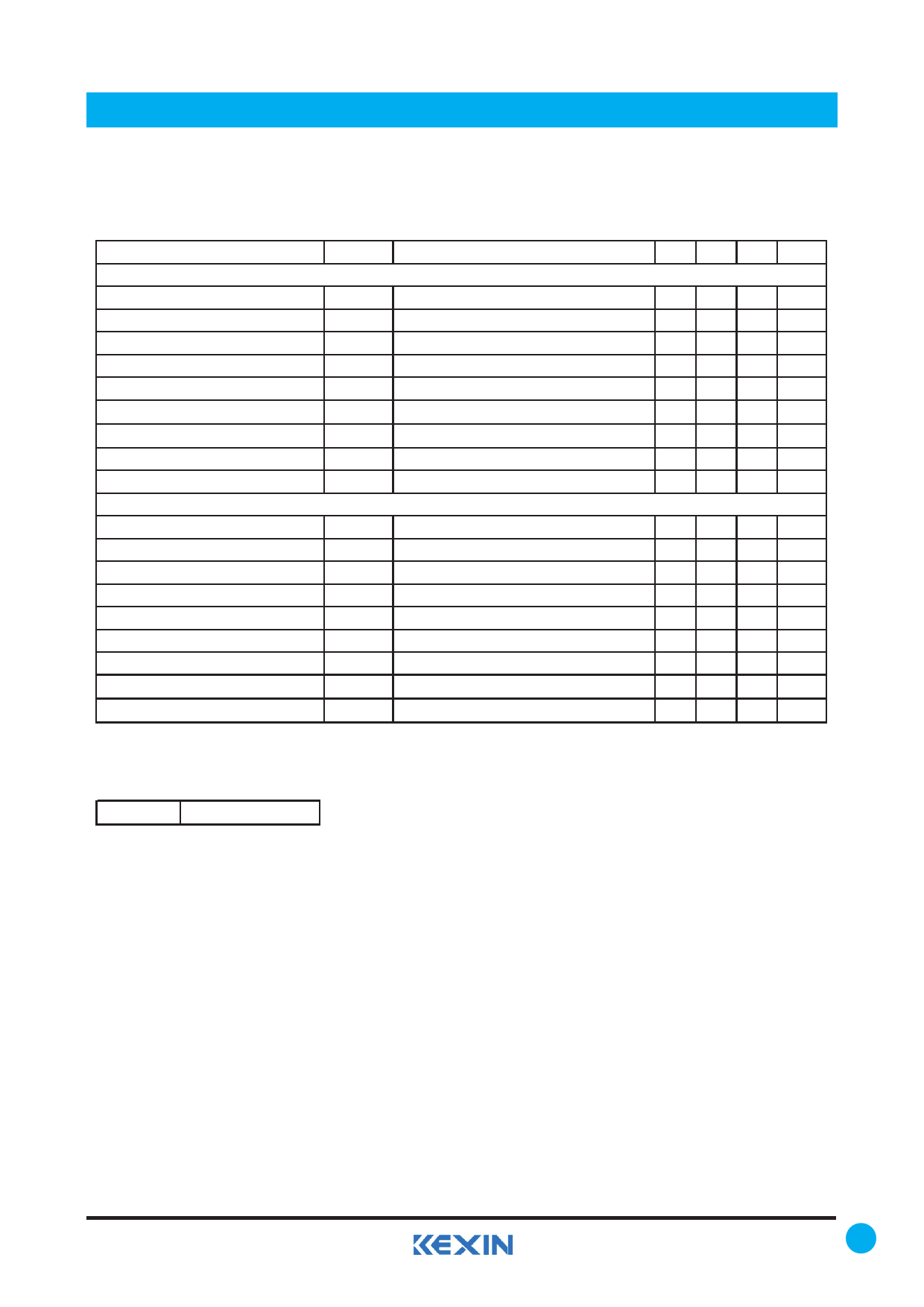
■ Electrical Characteristics Ta = 25℃
Parameter
Symbol
Test conditions
Transistor Tr1(PNP)
Collector-Base Breakdown Voltage
V(BR)CBO IC = -50 μA, IE = 0
Collector-Emitter Breakdown Voltage
V(BR)CEO IC = -1 mA, IB = 0
Emitter-Base Breakdown Voltage
V(BR)EBO IC = -50 μA, IC = 0
Collector cutoff current
ICBO VCB=-60V, IE=0
Emitter cutoff current
IEBO VEB=-6V, IC=0
DC current gain
hFE VCE=-6V, IC= -1mA
collector-emitter saturation voltage *
Transition frequency
Collector output capacitance
Transistor Tr2(NPN)
VCE(sat)
fT
Cob
IC = -50 mA; IB = -5 mA
IC = -2 mA; VCE = -12 V; f = 100 MHz
VCB=-12V, IE=0A, f=1MHz
Collector-Base Breakdown Voltage
V(BR)CBO IC = 50 μA, IE = 0
Collector-Emitter Breakdown Voltage
V(BR)CEO IC = 1 mA, IB = 0
Emitter-Base Breakdown Voltage
V(BR)EBO IC = 50 μA, IC = 0
Collector cutoff current
ICBO VCB=60V, IE=0
Emitter cutoff current
IEBO VEB=7V, IC=0
DC current gain
hFE VCE=6V, IC= 1mA
collector-emitter saturation voltage *
Transition frequency
Collector output capacitance
VCE(sat)
fT
Cob
IC = 50 mA; IB = 5 mA
IC = 2 mA; VCE = 12 V; f = 100 MHz
VCB=12V, IE=0A, f=1MHz
* pulse test: Pulse Width ≤300μs, Duty Cycle≤ 2.0%.
■ Marking
Marking
Y1
TransistIoCrs
Min Typ Max Unit
-60
V
-50
V
-6
V
-100 nA
-100 nA
120
560
-0.5 V
140
MHz
5
pF
60
V
50
V
7
V
100 nA
100 nA
120
560
0.4 V
180
MHz
3.5 pF
2
www.kexin.com.cn
Share Link: 