FPF1003A 查看數據表(PDF) - ON Semiconductor
零件编号
产品描述 (功能)
生产厂家
FPF1003A Datasheet PDF : 13 Pages
| |||
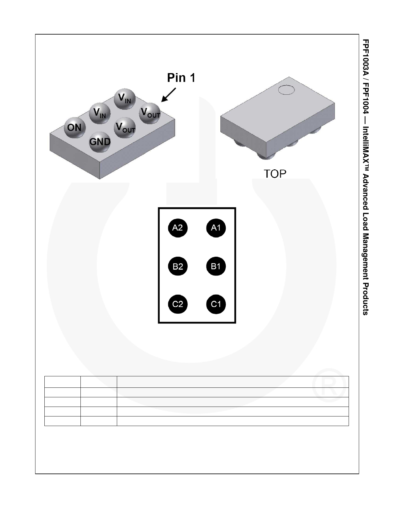
Pin Configurations
Figure 3. WLCSP Bumps Facing UP
Figure 4. WLCSP Bumps Facing Down
Figure 5. 1.0mm x 1.5mm WLCSP Pin Assignments (Bottom View)
Pin Definitions
Pin #
A2, B2
C2
A1, B1
C1
Name
VIN
ON
VOUT
GND
Description
Input to the power switch and the supply voltage for the IC
ON Control Input
Output of the power switch
Ground
© 2007 Fairchild Semiconductor Corporation
FPF1003A / FPF1004 • Rev. 1.0.6
3
www.fairchildsemi.com
Share Link: 