MC74LVX132 查看數據表(PDF) - ON Semiconductor
零件编号
产品描述 (功能)
生产厂家
MC74LVX132 Datasheet PDF : 7 Pages
| |||
MC74LVX132
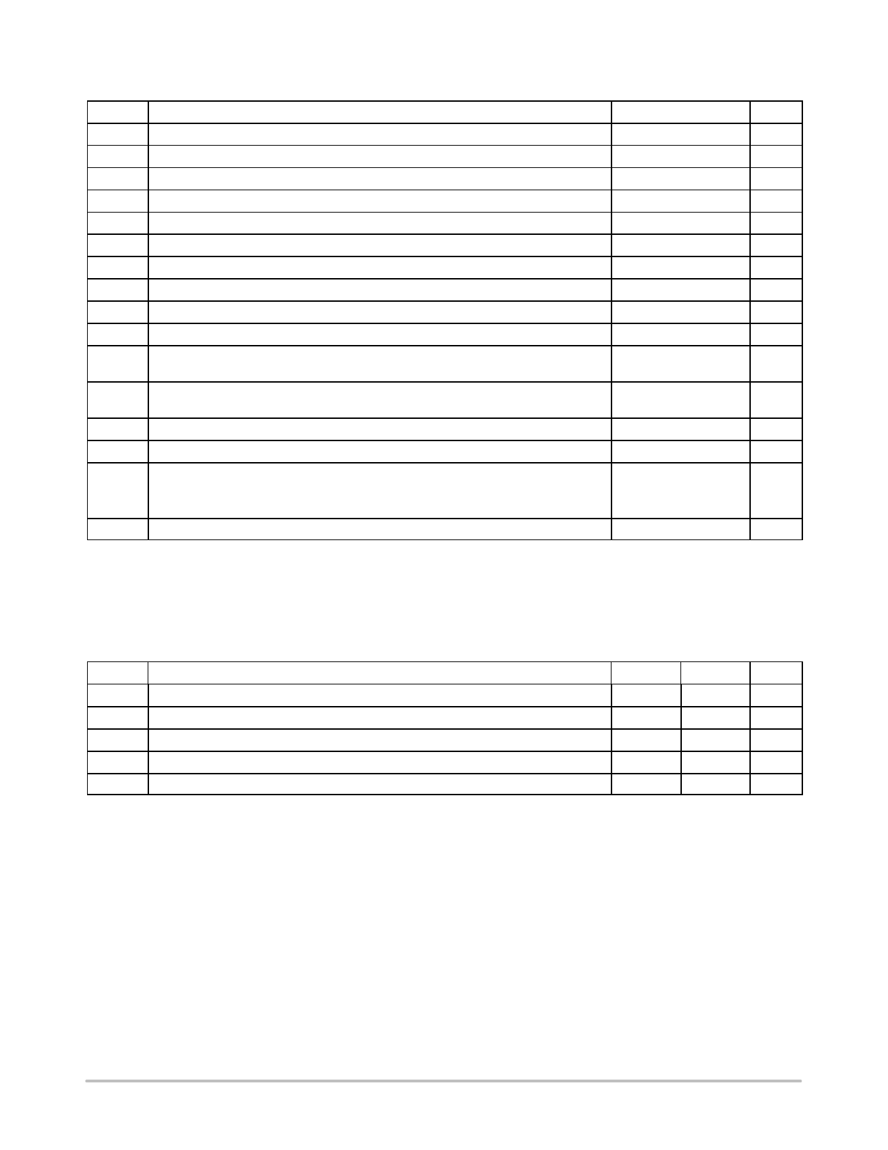
MAXIMUM RATINGS
Symbol
Parameter
Value
Unit
VCC
VIN
VOUT
IIK
IOK
IOUT
ICC
TSTG
TL
TJ
qJA
DC Supply Voltage
DC Input Voltage
DC Output Voltage
DC Input Diode Current
DC Output Diode Current
DC Output Sink Current
DC Supply Current per Supply Pin
Storage Temperature Range
Lead Temperature, 1 mm from Case for 10 Seconds
Junction Temperature under Bias
Thermal Resistance
VI < GND
VO < GND
SOIC
TSSOP
−0.5 to )7.0
−0.5 to )7.0
−0.5 to VCC )0.5
−20
±20
±25
±50
−65 to )150
260
)150
250
V
V
V
mA
mA
mA
mA
_C
_C
_C
_C/W
PD
Power Dissipation in Still Air at 85_C
SOIC
250
mW
TSSOP
MSL Moisture Sensitivity
Level 1
FR
VESD
Flammability Rating
ESD Withstand Voltage
Oxygen Index: 30% − 35% UL 94−V0 @ 0.125 in
Human Body Model (Note 1)
> 2000
V
Machine Model (Note 2)
> 200
Charged Device Model (Note 3)
N/A
ILatchup Latchup Performance
Above VCC and Below GND at 85_C (Note 4)
±300
mA
Stresses exceeding those listed in the Maximum Ratings table may damage the device. If any of these limits are exceeded, device functionality
should not be assumed, damage may occur and reliability may be affected.
1. Tested to EIA/JESD22−A114−A.
2. Tested to EIA/JESD22−A115−A.
3. Tested to JESD22−C101−A.
4. Tested to EIA/JESD78.
RECOMMENDED OPERATING CONDITIONS
Symbol
Parameter
Min
Max
Unit
VCC Supply Voltage
2.0
3.6
V
VI
Input Voltage
(Note 5)
0
5.5
V
VO
Output Voltage
(HIGH or LOW State)
0
5.5
V
TA
Operating Free−Air Temperature
*40
)125
_C
Dt/DV Input Transition Rise or Fall Rate
VCC = 3.0 V $0.3 V
0
100
ns/V
Functional operation above the stresses listed in the Recommended Operating Ranges is not implied. Extended exposure to stresses beyond
the Recommended Operating Ranges limits may affect device reliability.
5. Unused inputs may not be left open. All inputs must be tied to a high− or low−logic input voltage level.
http://onsemi.com
2
Share Link: 