ISL36111DRZ-T7 查看數據表(PDF) - Renesas Electronics
零件编号
产品描述 (功能)
生产厂家
ISL36111DRZ-T7 Datasheet PDF : 9 Pages
| |||
ISL36111
Electrical Specifications VDD = 1.2V, TA = +25°C, and VIN = 600mVP-P, unless otherwise noted. (Continued)
PARAMETERS
SYMBOL
CONDITION
MIN
MAX
(Note 14) TYP (Note 14) UNITS NOTES
Output Residual Jitter
10.3125Gbps; Up to 10m 28AWG standard twin-
axial cable (approx. -27dB @ 5GHz)
0.35
UI 6, 11, 12
Output Transition Time
Propagation Delay
tr, tf 20% to 80%
From IN to OUT
32
ps
13
500
ps
NOTES:
6. The input pins IN[P,N] are DC biased to VDD. The specified cable input amplitude range is established by characterization and not production tested,
and is valid so long as the voltages at the input pins IN[P,N] do not violate the voltage ranges specified in “Absolute Maximum Ratings” on page 3.
7. Maximum Reflection Coefficient given by equation SDDXX(dB) = -12 + 2*(f), with f in GHz. Established by characterization and not production tested.
8. Maximum Reflection Coefficient given by equation SDDXX(dB) = -6.3 + 13Log10(f/5.5), with f in GHz. Established by characterization and not
production tested.
9. Reflection Coefficient given by equation SCCXX(dB) < -7 + 1.6*f, with f in GHz. Established by characterization and not production tested.
10. Limits established by characterization and are not production tested.
11. Output residual jitter is the difference between the total jitter at the lane extender output and the total jitter of the transmitted signal (as measured
at the input to the channel). Total jitter (TJ) is DJpp + 14.1 x RJRMS
12. Measured using a PRBS 215-1 pattern. Deterministic jitter at the input to the lane extender is due to frequency-dependent, media-induced loss only.
13. Rise and fall times measured using a 2GHz clock with a 20ps edge rate.
14. Compliance to limits is assured by characterization and design.
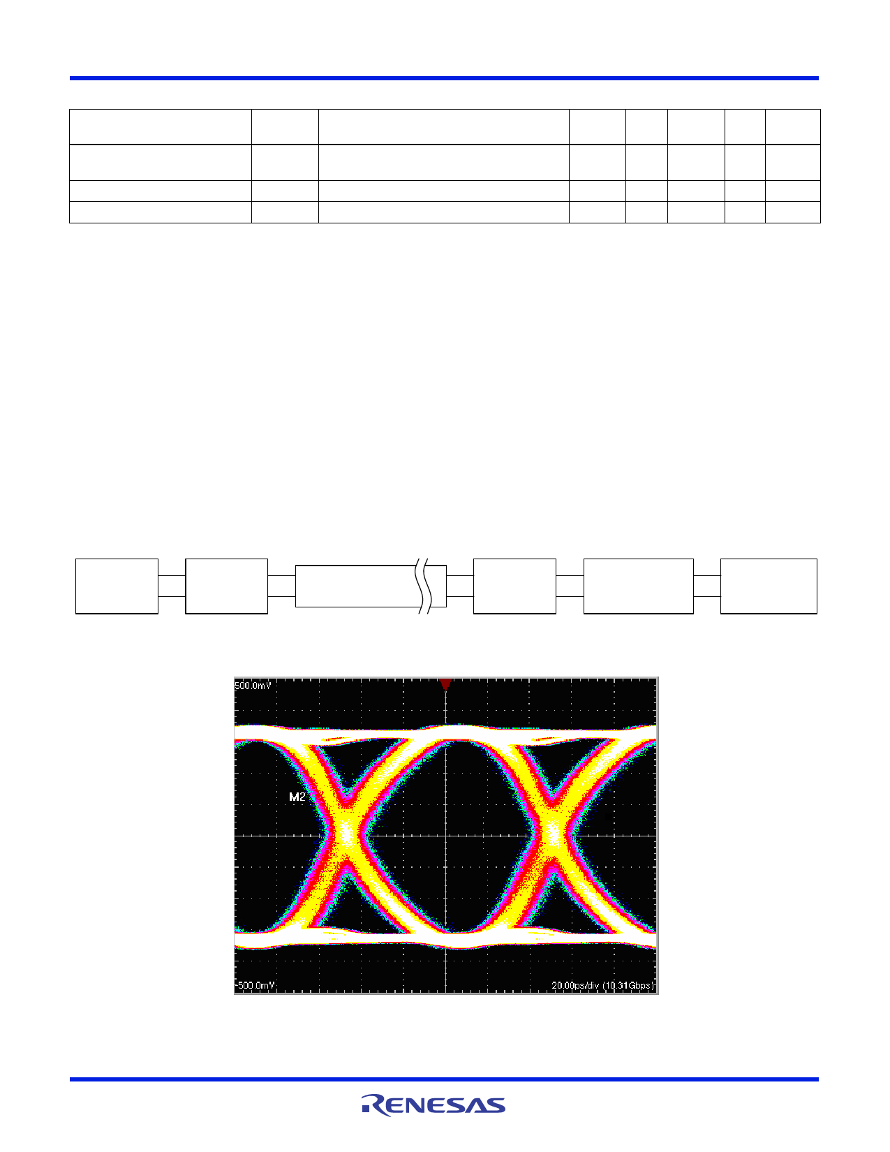
Typical Performance Characteristics
Performance is measured using the test setup illustrated in Figure 2. The signal from the pattern generator is launched into the twin-ax
cable using an SMA adapter card. The chip evaluation board is connected to the output of the cable through another adapter card. The
ISL36111 output signal is then visualized on a scope to determine signal integrity parameters such as jitter.
Pattern
Generator
SMA
Adapter
Card
100O Twin-Axial
Cable
SMA
Adapter
Card
FIGURE 2. DEVICE CHARACTERIZATION SET UP
ISL36111 Eval
Board
Oscilloscope
FN6974 Rev 2.00
Jul 12, 2012
FIGURE 3. ISL36111 10.3125Gb/s OUTPUT FOR A 10M 28AWG CABLE
Page 4 of 9
Share Link: 