BTS542D2 查看數據表(PDF) - Siemens AG
零件编号
产品描述 (功能)
生产厂家
BTS542D2 Datasheet PDF : 13 Pages
| |||
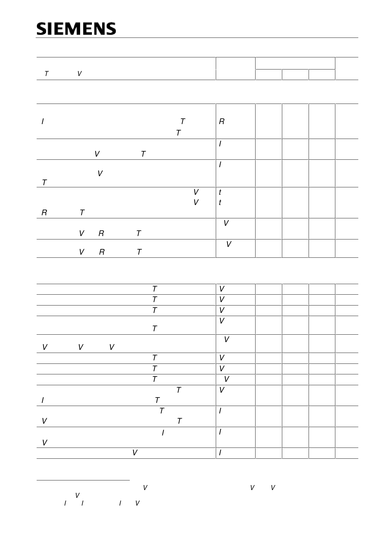
Electrical Characteristics
Parameter and Conditions
at Tj = 25 °C, Vbb = 12 V unless otherwise specified
BTS 542 D2
Symbol
Values
Unit
min typ max
Load Switching Capabilities and Characteristics
On-state resistance (pin 3 to 5)
IL = 5 A
Tj=25 °C: RON
-- 15 18 mW
Tj=150 °C:
28 35
Nominal load current (pin 3 to 5)
IL(ISO)
17 21
-- A
ISO Proposal: VON = 0.5 V, TC = 85 °C
Output current (pin 5) while GND disconnected or IL(GNDhigh)
--
GND pulled up, VIN= 0, see diagram page 7,
Tj =-40...+150°C
Turn-on time
to 90% VOUT: ton
100
Turn-off time
to 10% VOUT: toff
10
RL = 12 W, Tj =-40...+150°C
Slew rate on
10 to 30% VOUT, RL = 12 W, Tj =-40...+150°C
dV /dton
0.2
Slew rate off
70 to 40% VOUT, RL = 12 W, Tj =-40...+150°C
-dV/dtoff
0.4
--
1 mA
-- 350 ms
-- 130
--
2 V/ms
--
5 V/ms
Operating Parameters
Operating voltage 4)
Tj =-40...+150°C:
Undervoltage shutdown
Tj =-40...+150°C:
Undervoltage restart
Tj =-40...+150°C:
Undervoltage restart of charge pump
see diagram page 12
Tj =-40...+150°C:
Undervoltage hysteresis
DVbb(under) = Vbb(u rst) - Vbb(under)
Overvoltage shutdown
Tj =-40...+150°C:
Overvoltage restart
Tj =-40...+150°C:
Overvoltage hysteresis
Overvoltage protection5)
Ibb=40 mA
Tj =-40...+150°C:
Tj =-40°C:
Tj =25...+150°C:
Standby current (pin 3)
VIN=0, IST=0,
Tj=-40...+25°C:
Tj=150°C:
Leakage output current (included in Ibb(off))
VIN=0
Operating current (Pin 1)6), VIN=5 V
Vbb(on)
Vbb(under)
Vbb(u rst)
Vbb(ucp)
DVbb(under)
Vbb(over)
Vbb(o rst)
DVbb(over)
Vbb(AZ)
Ibb(off)
IL(off)
IGND
4.5
-- 42 V
2.4
-- 4.5 V
--
-- 4.5 V
-- 6.5 7.5 V
-- 0.2
-- V
42
--
42
--
-- 0.2
60
--
63 67
-- 12
-- 18
--
6
52 V
-- V
-- V
-- V
25 mA
60
-- mA
-- 1.1
-- mA
» 4) At supply voltage increase up to Vbb= 6.5 V typ without charge pump, VOUT Vbb - 2 V
5) see also VON(CL) in table of protection functions and circuit diagram page 7. Meassured without load.
6) Add IST, if IST > 0, add IIN, if VIN>5.5 V
Semiconductor Group
Page 3
13.Nov.95
Share Link: 