M5M51016BRT-10VL 查看數據表(PDF) - MITSUBISHI ELECTRIC
零件编号
产品描述 (功能)
生产厂家
M5M51016BRT-10VL
MITSUBISHI ELECTRIC

M5M51016BRT-10VL Datasheet PDF : 7 Pages
| |||
9 Jul ,1997
MITSUBISHI LSIs
M5M51016BTP,RT-10VL,
-10VLL
1048576-BIT(65536-WORD BY 16-BIT)CMOS STATIC RAM
FUNCTION
The operation mode of the M5M51016B series are determined by a
combination of the device control inputs BC1, BC2, CS, W and OE.
Each mode is summarized in the function table.
A write cycle is executed whenever the low level W overlaps with the
low level BC1 and/or BC2 and the high level CS. The address must be
set up before the write cycle and must be stable during the entire cycle.
The data is latched into a cell on the trailing edge of W, BC1, BC2 or
CS, whichever occurs first, requiring the set-up and hold time relative
to these edge to be maintained. The output enable input OE directly
controls the output stage. Setting the OE at a high level, the output stage
is in a high-impedance state, and the databus contention problem in the
write cycle is eliminated.
A read cycle is executed by setting W at a high level and OE at a low
level while BC1 and/or BC2 and CS are in an active state. (BC1
and/or BC2=L,CS=H)
When setting BC1 at a high level and the other pins are in an active
state, upper-Byte are in a selectable mode in which both reading and
writing are enabled, and lower-Byte are in a non-selectable mode.And
when setting BC2 at a high level and the other pins are in an active
state, lower-Byte are in a selectable mode and upper -Byte are in a
non-selectable mode.
When setting BC1 and BC2 at a high level or CS at a low level, the chips
are in a non-selectable mode in which both reading and writing are
disabled.
In this mode, the output stage is in a high-impedance state, allowing OR-
tie with other chips and memory expansion by BC1, BC2 and CS. The
power supply current is reduced as low as the stand-by current which is
specified as ICC3 or ICC4, and the memory data can be held at +2V power
supply, enabling battery back-up operation during powerfailure or power-
down operation in the non-selected mode.
CS BC1 BC2 W OE Mode
DQ1~8 DQ9~16 ICC
L X X X X Non selection High-Z High-Z Stand-by
X H H X X Non selection High-Z High-Z Stand-by
H H L L X Upper-Byte Write High-Z Din
Active
H H L H L Upper-Byte Read High-Z Dout Active
H HL HH
High-Z High-Z Active
H L H L X Lower-Byte Write Din High-Z Active
H L H H L Lower-Byte Read Dout High-Z Active
H L HHH
High-Z High-Z Active
H L L L X Word Write Din
Din Active
H L L H L Word Read Dout Dout Active
H L L HH
High-Z High-Z Active
(High-Z=High-impedance)
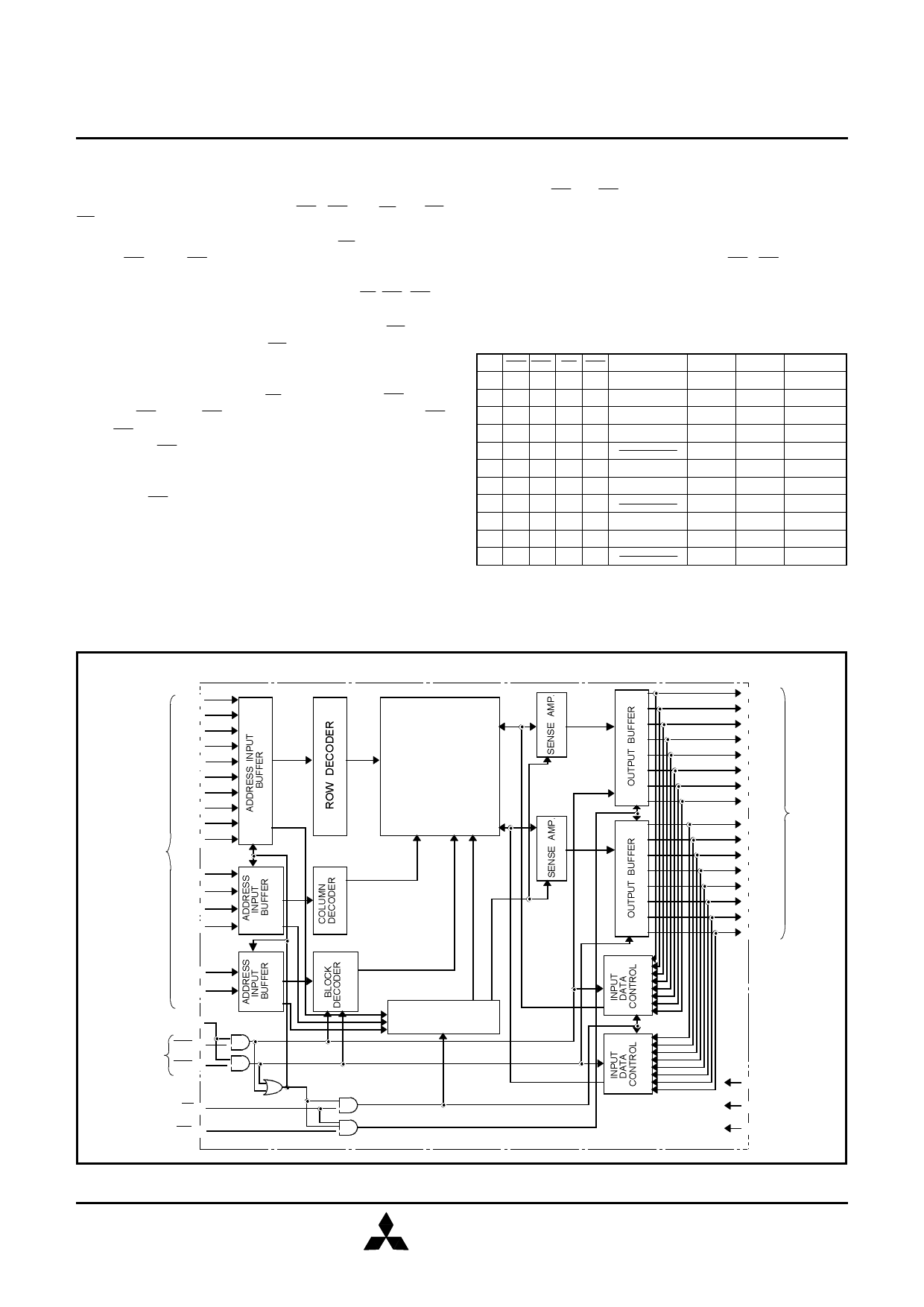
BLOCK DIAGRAM
ADDRESS
INPUTS
A1 9
A3 7
A6 4
A7 3
A12 2
A14 41
A1540
A13 39
A8 37
A9 36
A0 10
A4 6
A2 8
A5 5
A10 34
A11 35
CHIP SELECT
INPUT
BYTE
CONTROL
INPUTS
CS 11
BC1 43
BC2 42
WRITE CONTROL
INPUT
W 38
OUTPUT ENABLE
INPUT
OE 13
65536 WORDS x16 BITS
( 1024 ROWS
x 256 COLUMNS
x 4 BLOCKS )
CLOCK
GENERATOR
MITSUBISHI
ELECTRIC
15 DQ1
16 DQ2
17 DQ3
18 DQ4
19 DQ5
20 DQ6
21 DQ7
22 DQ8
24 DQ9
25 DQ10
26 DQ11
27 DQ12
28 DQ13
29 DQ14
30 DQ15
31 DQ16
DATA
INPUTS/
OUTPUTS
23 Vcc
33 GND(0V)
12 GND (0V)
2
Share Link: