WED3EG6417S-D4 查看數據表(PDF) - White Electronic Designs Corporation
零件编号
产品描述 (功能)
生产厂家
WED3EG6417S-D4 Datasheet PDF : 7 Pages
| |||
White Electronic Designs
WED3EG6417S-D4
*ADVANCED
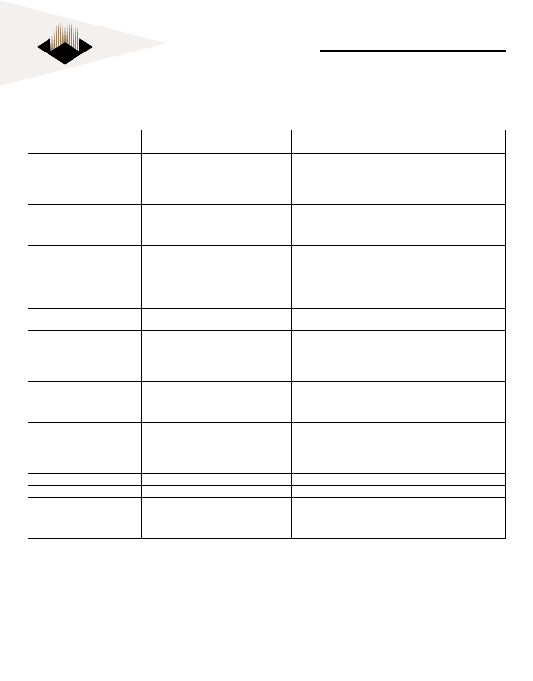
IDD SPECIFICATIONS AND TEST CONDITIONS
(Recommended operating conditions, TA = 0 to 70°C, VCCQ = 2.5V ±0.2V, VCC = 2.5V ±0.2V)
Parameter
Symbol Conditions
Operating Current
One device bank; Active = Precharge;
tRC=tRC(MIN); tCK=tCK
IDD0 (MIN); DQ, DM and DQS inputs changing
once per clock cycle; Address and control
inputs changing once every two cycles.
Operating Current
One device banks; Active-Read-Precharge;
IDD1
Burst = 2; tRC=tRC(MIN); tCK=tCK
(MIN); lout=0mA; Address and control inputs
changing once per clock cycle.
Precharge Power-
Down Standby Current
IDD2P
All device bank idle; Power-down mode;
tCK=tCK(MIN); CKE=(low)
Idle Standby Current
Active Power-Down
Standby Current
CS# = High; All device banks idle; tCK=tCK(MIN);
IDD2F
CKE = high; Address and other control inputs
changing once per clock cycle. VIN = VREF for
DQ, DQS and DM.
IDD3P
One device bank active; Power-down mode;
tCK(MIN); CKE=(low)
CS# = High; CKE = High; One device bank;
Active-Precharge; tRC=tRAS(MAX); tCK=tCK(MIN);
Active Standby Current IDD3N DQ, DM and DQS inputs changing twice per
clock cycle; Address and other control inputs
changing once per clock cycle
Operating Current
Burst = 2; Reads; Continous burst; Once
IDD4R
device bank active; Address and control inputs
changing once per clock cycle; tCK=tCK(MIN);
IOUT=0mA
Operating Current
Auto Refresh Current
Self Refresh Current
Burst=2; Writes; Continous burst; Once device
bank active; Address and control inputs
IDD4W changing once per clock cycle; tCK=tCK(MIN);
DQ,DM and DQS inputs changing twice per
clock cycle.
IDD5
tRC=tRC(MIN)
IDD6 CKE £ 0.2V
Operating Current
Four bank interleaving Reads (BL=4) with
IDD7A
auto precharge with tRC=tRC(MIN); tCK=tCK(MIN);
Address and control input change only during
Active Read or Write commands.
DDR266@CL=2
Max
DDR266@CL=2.5
Max
DDR200@CL=2
Max
Units
680
680
600
mA
880
880
800
mA
32
32
28
mA
200
200
176
mA
280
280
280
mA
400
400
360
mA
1360
1360
1160
mA
1400
1400
1120
mA
1520
1520
1280
mA
16
16
16
mA
2640
2640
2080
mA
* Mode IDD was calculeter on the basis of component IDD and can be differently measured according to DQ loading cap.
White Electronic Designs Corp. reserves the right to change products or specifications without notice.
March 2002
Rev. # 0
5
White Electronic Designs Corporation • (602) 437-1520 • www.wedc.com
Share Link: 