NES2427P-45 查看數據表(PDF) - NEC => Renesas Technology
零件编号
产品描述 (功能)
生产厂家
NES2427P-45 Datasheet PDF : 8 Pages
| |||
NES2427P-45
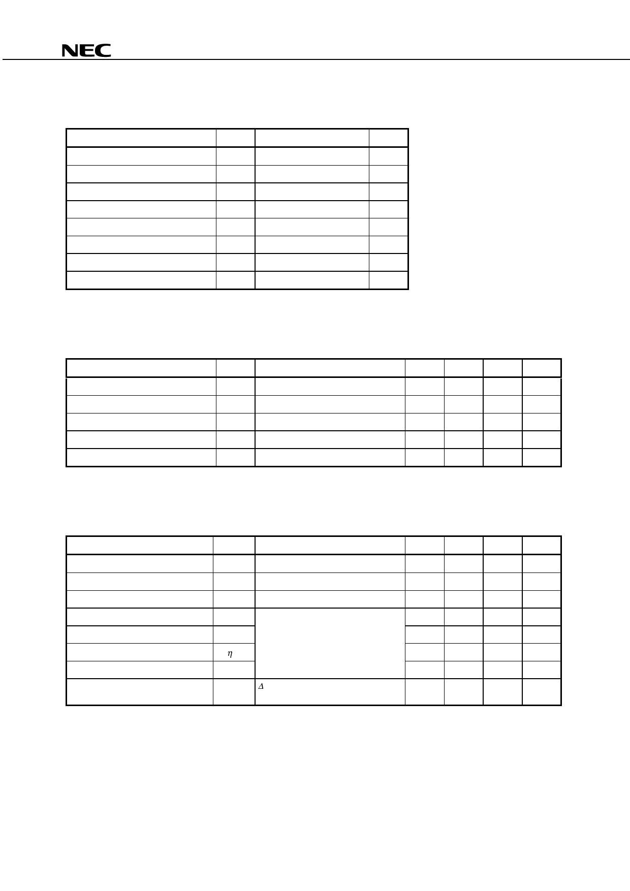
ABSOLUTE MAXIMUM RATINGS (Unless otherwise specified, TA = +25 °C)
Operation in excess of any one of these parameters may result in permanent damage.
Parameter
Drain to Source Voltage
Gate to Source Voltage
Gate to Drain Voltage
Drain Current
Gate Current
Total Power Dissipation
Channel Temperature
Storage Temperature
Symbol
Ratings
Unit
VDS
19
V
VGSO
−7
V
VGDO
−22
V
ID
24
A
IG
240
mA
P Note
tot
165
W
Tch
175
°C
Tstg
−65 to +175
°C
Note TC = +25 °C
RECOMMENDED OPERATING CONDITIONS
Parameter
Drain to Source Voltage
Gain Compression
Channel Temperature
Set Drain Current
Gate Resistance
Symbol
Test Conditions
VDS
Gcomp
Tch
IDset
R Note
g
VDS = 12.0 V, RF OFF
MIN. TYP. MAX. Unit
−
−
12.0
V
−
−
3.0
dB
−
−
+150
°C
−
4.0
6.0
A
−
−
30
Ω
Note Rg is the series resistance between the gate supply and the FET gate.
ELECTRICAL CHARACTERISTICS (TA = +25 °C)
Parameter
Saturated Drain Current
Pinch-off Voltage
Thermal Resistance
Output Power
Drain Current
Power Added Efficiency
Linear Gain
3rd Order Intermodulation Distortion
Symbol
Test Conditions
IDSS VDS = 2.5 V, VGS = 0 V
Vp VDS = 2.5 V, ID = 110 mA
Rth Channel to Case
Pout
ID
ηadd
G Note2
L
IM3
f = 2.70 GHz, VDS = 12.0 V,
Pin = 38.5 dBm, Rg = 30 Ω,
IDset = 4.0 A Total (RF OFF) Note1
∆f = 5 MHz,
Pout = 37 dBm (2 tones total)
MIN.
−
−4.0
−
45.5
−
−
10
−
TYP.
24.0
−2.6
0.7
46.5
8
41
11
−38
MAX.
−
−
0.9
−
−
−
−
−
Unit
A
V
°C/W
dBm
A
%
dB
dBc
Notes 1. IDset = 2.0 A each drain
2. Pin = 22 dBm
2
Preliminary Data Sheet P14810EJ1V0DS00
Share Link: 