NVTA7002N(2012) 查看數據表(PDF) - ON Semiconductor
零件编号
产品描述 (功能)
生产厂家
NVTA7002N
(Rev.:2012)
(Rev.:2012)
ON Semiconductor

NVTA7002N Datasheet PDF : 5 Pages
| |||
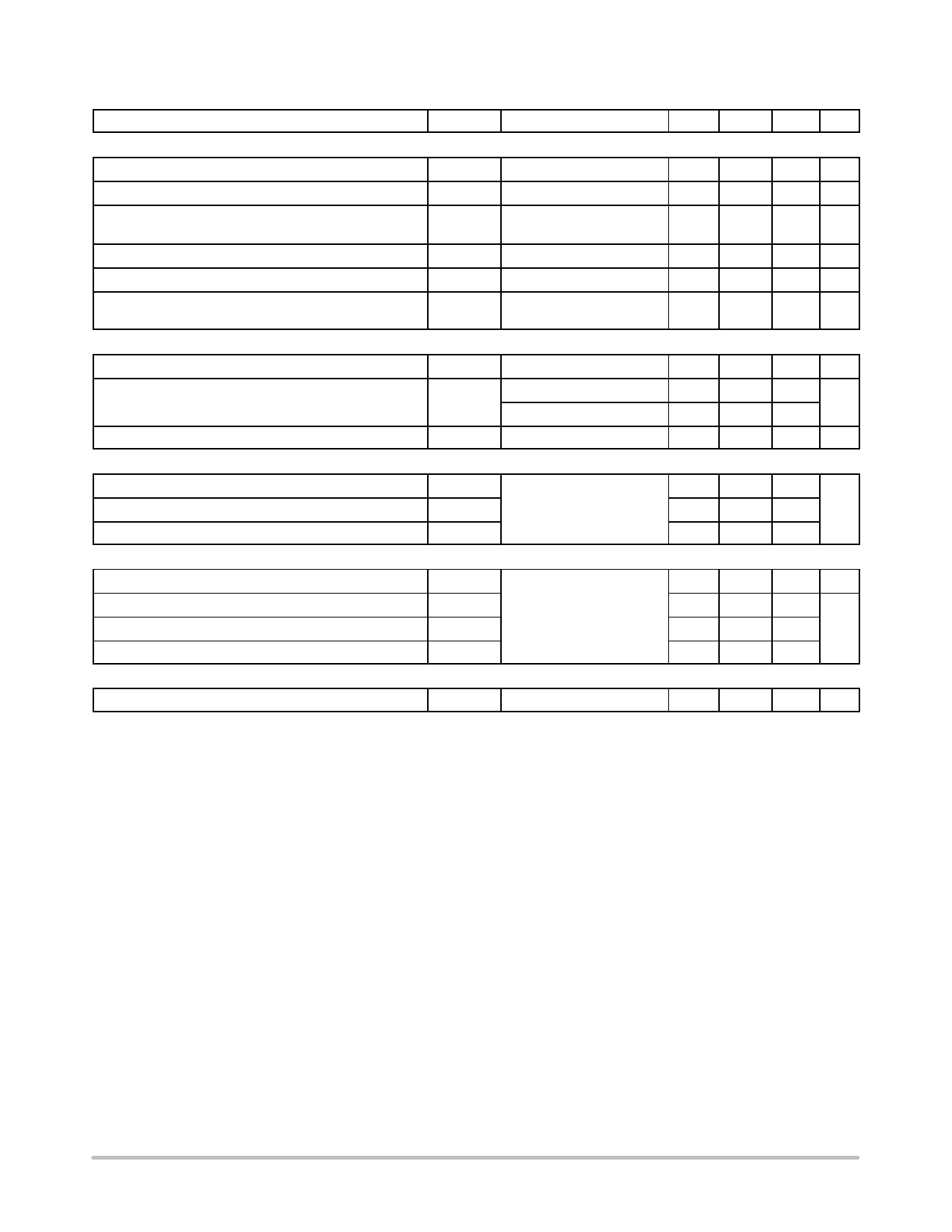
NTA7002N, NVTA7002N
ELECTRICAL CHARACTERISTICS (TJ = 25°C unless otherwise specified)
Parameter
Symbol
Test Condition
Min Typ Max Unit
OFF CHARACTERISTICS
Drain−to−Source Breakdown Voltage
Zero Gate Voltage Drain Current
Zero Gate Voltage Drain Current
V(BR)DSS
VGS = 0 V, ID = 100 mA
30
IDSS
VGS = 0 V, VDS = 30 V
IDSS
VGS = 0 V, VDS = 20 V,
T = 85 °C
V
1.0 mA
1.0 mA
Gate−to−Source Leakage Current
Gate−to−Source Leakage Current
Gate−to−Source Leakage Current
IGSS
IGSS
IGSS
VDS = 0 V, VGS = ±10 V
VDS = 0 V, VGS = ±5 V
VDS = 0 V, VGS = ±5 V
T = 85 °C
±25 mA
±1.0 mA
±1.0 mA
ON CHARACTERISTICS (Note 2)
Gate Threshold Voltage
Drain−to−Source On Resistance
Forward Transconductance
CAPACITANCES
VGS(TH)
VDS = VGS, ID = 100 mA
0.5
1.0
1.5 V
RDS(on)
VGS = 4.5 V, ID = 154 mA
VGS = 2.5 V, ID = 154 mA
1.4
7.0
W
2.3
7.5
gFS
VDS = 3 V, ID = 154 mA
80
mS
Input Capacitance
Output Capacitance
Reverse Transfer Capacitance
SWITCHING CHARACTERISTICS (Note 3)
CISS
COSS
CRSS
VDS = 5.0 V, f = 1 MHz,
VGS = 0 V
11.5 20
10
15 pF
3.5
6.0
Turn−On Delay Time
Rise Time
Turn−Off Delay Time
Fall Time
DRAIN−SOURCE DIODE CHARACTERISTICS
td(ON)
tr
td(OFF)
tf
VGS = 4.5 V, VDS = 5.0 V,
ID = 75 mA, RG = 10 W
13
ns
15
98
ns
60
Forward Diode Voltage
VSD
VGS = 0 V, IS = 154 mA
2. Pulse Test: pulse width v 300 ms, duty cycle v 2%.
3. Switching characteristics are independent of operating junction temperatures.
0.77 0.9 V
http://onsemi.com
2
Share Link: