OR3C55 ТЪЦуюІТЋИТЊџУАе№╝ѕPDF№╝Ѕ - Agere -> LSI Corporation
жЏХС╗Ху╝ќтЈи
С║ДтЊЂТЈЈУ┐░ (тіЪУЃй)
ућЪС║Дтјѓт«Х
OR3C55 Datasheet PDF : 210 Pages
| |||
ORCA Series 3C and 3T FPGAs
Data Sheet
June 1999
System-Level Features
System-level features reduce glue logic requirements
and make a system on a chip possible. These features
in the ORCA Series 3 include:
s Full PCI local bus compliance.
s Dual-use microprocessor interface (MPI) can be
used for configuration, readback, device control, and
device status, as well as for a general-purpose inter-
face to the FPGA. Glueless interface to i960* and
PowerPCРђа processors with user-configurable
address space provided.
s Parallel readback of configuration data capability with
the built-in microprocessor interface.
s Programmable clock manager (PCM) adjusts clock
phase and duty cycle for input clock rates from
5 MHz to 120 MHz. The PCM may be combined with
FPGA logic to create complex functions, such as dig-
ital phase-locked loops (DPLL), frequency counters,
and frequency synthesizers or clock doublers. Two
PCMs are provided per device.
s True, internal, 3-state, bidirectional buses with simple
control provided by the SLIC.
s 32 x 4 RAM per PFU, configurable as single- or dual-
port at >176 MHz. Create large, fast RAM/ROM
blocks (128 x 8 in only eight PFUs) using the SLIC
decoders as bank drivers.
* i960 is a registered trademark of Intel Corporation.
Рђа PowerPC is a registered trademark of International Business
Machines Corporation.
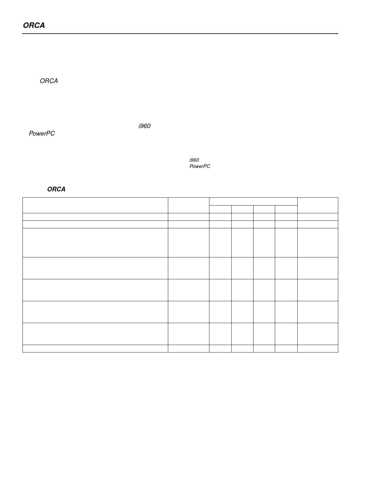
Table 2. ORCA Series 3 System Performance
Parameter
16-bit Loadable Up/Down Counter
16-bit Accumulator
8 x 8 Parallel Multiplier:
Multiplier Mode, Unpipelined1
ROM Mode, Unpipelined2
Multiplier Mode, Pipelined3
32 x 16 RAM (synchronous):
Single-port, 3-state Bus4
Dual-port5
128 x 8 RAM (synchronous):
Single-port, 3-state Bus4
Dual-port5
8-bit Address Decode (internal):
Using Softwired LUTs
Using SLICs6
32-bit Address Decode (internal):
Using Softwired LUTs
Using SLICs7
36-bit Parity Check (internal)
# PFUs
2
2
11.5
8
15
4
4
8
8
0.25
0
2
0
2
Speed
-4
-5
-6
-7
78 102 131 168
78 102 131 168
19
25
30
38
51
66
80 102
76 104 127 166
97 127 151 192
127 166 203 253
88 116 139 176
88 116 139 176
4.87 3.66 2.58 2.03
2.35 1.82 1.23 0.99
16.06 12.07 9.01 7.03
6.91 5.41 4.21 3.37
16.06 12.07 9.01 7.03
Unit
MHz
MHz
MHz
MHz
MHz
MHz
MHz
MHz
MHz
ns
ns
ns
ns
ns
1. Implemented using 8 x 1 multiplier mode (unpipelined), register-to-register, two 8-bit inputs, one 16-bit output.
2. Implemented using two 32 x 12 ROMs and one 12-bit adder, one 8-bit input, one fixed operand, one 16-bit output.
3. Implemented using 8 x 1 multiplier mode (fully pipelined), two 8-bit inputs, one 16-bit output (7 of 15 PFUs contain only pipelining registers).
4. Implemented using 32 x 4 RAM mode with read data on 3-state buffer to bidirectional read/write bus.
5. Implemented using 32 x 4 dual-port RAM mode.
6. Implemented in one partially occupied SLIC with decoded output set up to CE in same PLC.
7. Implemented in five partially occupied SLICs.
6
Lucent Technologies Inc.
Share Link: 