PACDN009 查看數據表(PDF) - ON Semiconductor
零件编号
产品描述 (功能)
生产厂家
PACDN009 Datasheet PDF : 7 Pages
| |||
PACDN009
PERFORMANCE INFORMATION
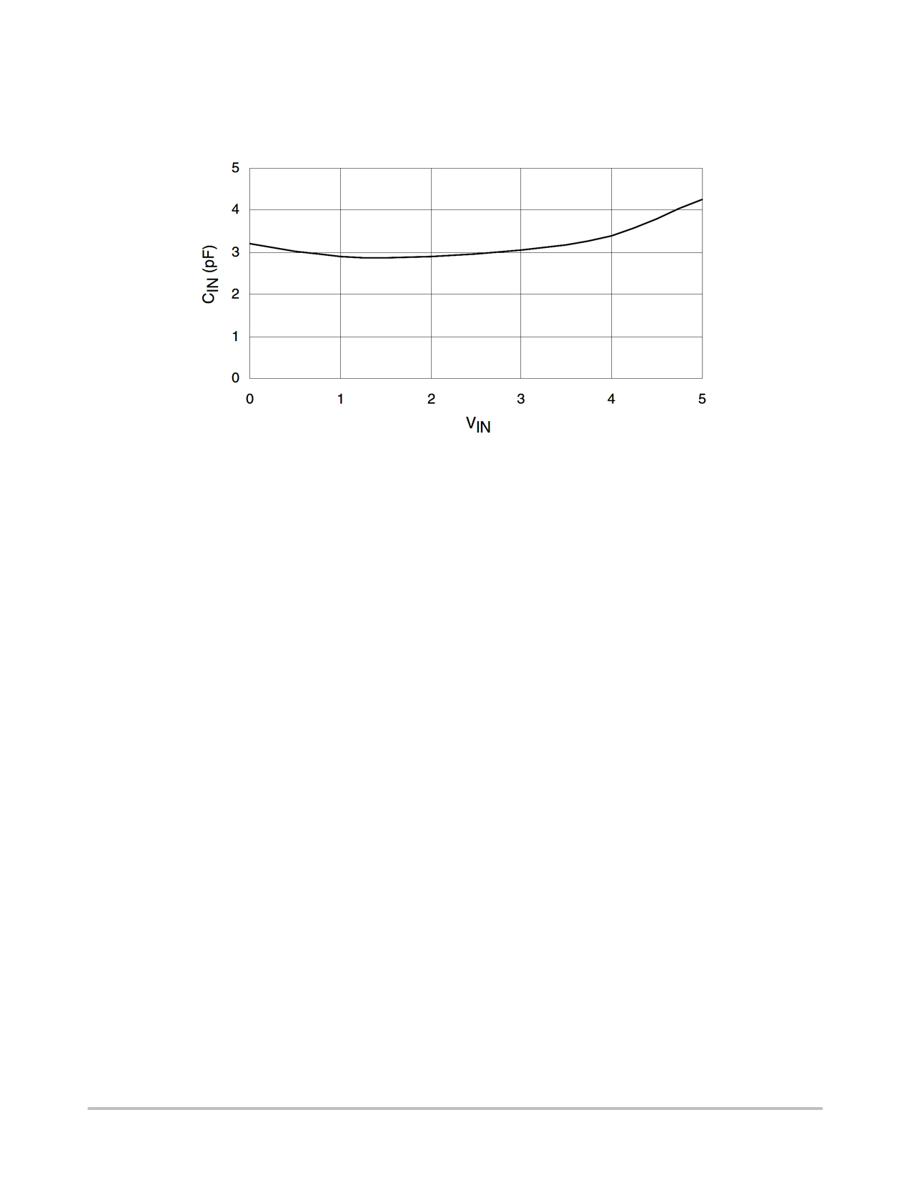
Input Capacitance vs. Input Voltage
Figure 1. Typical Variation of CIN vs. VIN
(VP = 5 V, VN = 0 V, 0.1 mF Chip Capacitor between VP and VN)
APPLICATION INFORMATION
Design Considerations
In order to realize the maximum protection against ESD pulses, care must be taken in the PCB layout to minimize parasitic
series inductances on the Supply/Ground rails as well as the signal trace segment between the signal input (typically
a connector) and the ESD protection device. Refer to Figure 2, which illustrates an example of a positive ESD pulse striking
an input channel. The parasitic series inductance back to the power supply is represented by L1 and L2. The voltage VCL on
the line being protected is:
VCL + Fwd Voltage Drop of D1 ) VSUPPLY ) L1 d(IESD)ńdt ) L2 d(IESD)ńdt
where IESD is the ESD current pulse, and VSUPPLY is the positive supply voltage.
An ESD current pulse can rise from zero to its peak value in a very short time. As an example, a level 4 contact discharge
per the IEC61000−4−2 standard results in a current pulse that rises from zero to 30 Amps in 1 ns. Here d(IESD)/dt can be
approximated by DIESD/Dt, or 30/(1x10−9). So just 10 nH of series inductance (L1 and L2 combined) will lead to a 300 V
increment in VCL!
Similarly for negative ESD pulses, parasitic series inductance from the VN pin to the ground rail will lead to drastically
increased negative voltage on the line being protected.
Another consideration is the output impedance of the power supply for fast transient currents. Most power supplies exhibit
a much higher output impedance to fast transient current spikes. In the VCL equation above, the VSUPPLY term, in reality, is
given by (VDC + IESD x ROUT), where VDC and ROUT are the nominal supply DC output voltage and effective output impedance
of the power supply respectively. As an example, a ROUT of 1 W would result in a 10 V increment in VCL for a peak IESD of
10 A.
If the inductances and resistance described above are close to zero, the rail−clamp ESD protection diodes will do a good job
of protection. However, since this is not possible in practical situations, a bypass capacitor must be used to absorb the very high
frequency ESD energy. So for any brand of rail−clamp ESD protection diodes, a bypass capacitor should be connected between
the VP pin of the diodes and the ground plane (VN pin of the diodes) as shown in the Application Circuit diagram below. A value
of 0.22 mF is adequate for IEC−61000−4−2 level 4 contact discharge protection (8 kV). Ceramic chip capacitors mounted with
short printed circuit board traces are good choices for this application. Electrolytic capacitors should be avoided as they have
poor high frequency characteristics. For extra protection, connect a zener diode in parallel with the bypass capacitor to mitigate
http://onsemi.com
4
Share Link: 