TISP3072F3D 查看數據表(PDF) - Bourns, Inc
零件编号
产品描述 (功能)
生产厂家
TISP3072F3D Datasheet PDF : 12 Pages
| |||
TISP30xxF3 (LV) Overvoltage Protector Series
APPLICATIONS INFORMATION
Protection Voltage
The
rate
protection
of current
voltage, (V(BO)
rise, di/dt, when
), increases under
the TISP® device
lightning surge
is clamping the
conditions
voltage in
due to thyristor regeneration. This increase is
its breakdown region. The V(BO) value under
dependent on the
surge conditions can
be estimated by multiplying the 50 Hz rate V(BO) (250 V/ms) value by the normalized increase at the surge’s di/dt (Figure 7). An estimate of the
di/dt can be made from the surge generator voltage rate of rise, dv/dt, and the circuit resistance.
As an example, the ITU-T K.21 1.5 kV, 10/700 µs surge has an average dv/dt of 150 V/µs, but, as the rise is exponential, the initial dv/dt is
higher, being in the region of 450 V/µs. The instantaneous generator output resistance is 25 Ω. If the equipment has an additional series
resistance of 20 Ω, the total series resistance becomes 45 Ω. The maximum di/dt then can be estimated as 450/45 = 10 A/µs. In practice, the
measured di/dt and protection voltage increase will be lower due to inductive effects and the finite slope resistance of the TISP® breakdown
region.
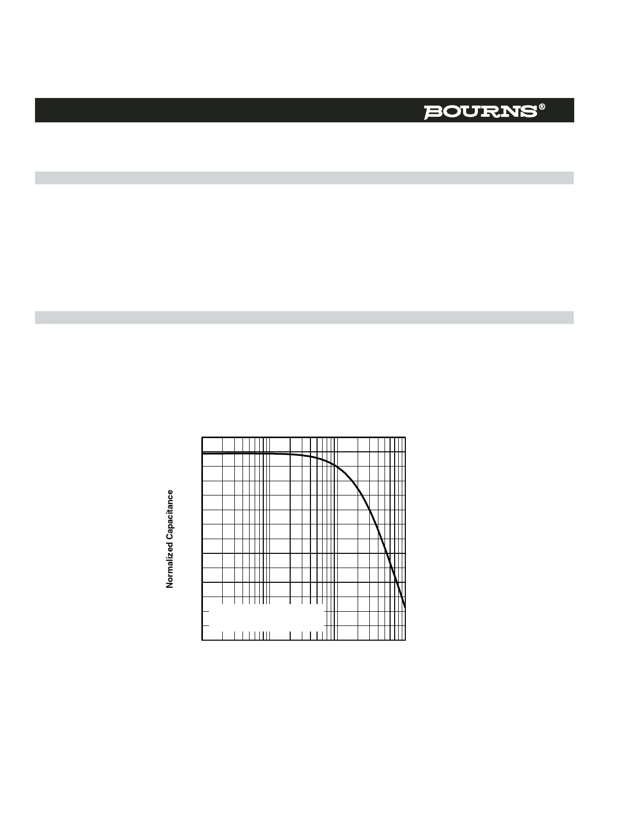
Capacitance
Off-state Capacitance
The off-state capacitance of a TISP® device is sensitive to junction temperature, TJ, and the bias voltage, comprising of the d.c. voltage, VD,
and the a.c. voltage, Vd. All the capacitance values in this data sheet are measured with an a.c. voltage of 100 mV. The typical 25 °C variation
of capacitance value with a.c. bias is shown in Figure 17. When VD >> Vd, the capacitance value is independent on the value of Vd. The
capacitance is essentially constant over the range of normal telecommunication frequencies.
1.05
NORMALIZED CAPACITANCE
vs
RMS AC TEST VOLTAGE
AIXXAA
1.00
0.95
0.90
0.85
0.80
0.75
Normalized to Vd = 100 mV
DC Bias, VD = 0
0.70
1
10
100
Vd - RMS AC Test Voltage - mV
Figure 17.
1000
MARCH 1994 - REVISED MARCH 2006
Specifications are subject to change without notice.
Customers should verify actual device performance in their specific applications.
Share Link: 