TISP3072F3DR 查看數據表(PDF) - Bourns, Inc
零件编号
产品描述 (功能)
生产厂家
TISP3072F3DR Datasheet PDF : 12 Pages
| |||
TISP30xxF3 (LV) Overvoltage Protector Series
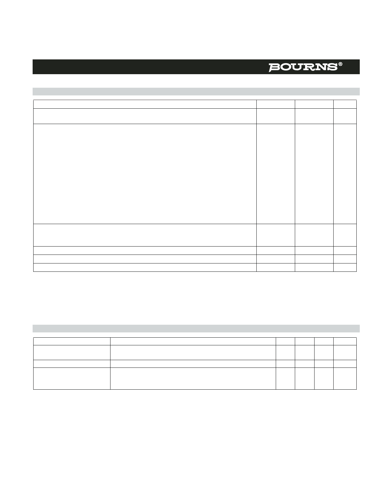
Absolute Maximum Ratings, TA = 25 °C (Unless Otherwise Noted)
Rating
Repetitive peak off-state voltage, 0 °C < TA < 70 °C
‘3072F3
‘3082F3
Non-repetitive peak on-state pulse current (see Notes 1 and 2)
1/2 (Gas tube differential transient, 1/2 voltage wave shape)
2/10 (Telcordia GR-1089-CORE, 2/10 voltage wave shape)
1/20 (ITU-T K.22, 1.2/50 voltage wave shape, 25 Ω resistor)
8/20 (IEC 61000-4-5, combination wave generator, 1.2/50 voltage wave shape)
10/160 (FCC Part 68, 10/160 voltage wave shape)
4/250 (ITU-T K.20/21, 10/700 voltage wave shape, simultaneous)
0.2/310 (CNET I 31-24, 0.5/700 voltage wave shape)
5/310 (ITU-T K.20/21, 10/700 voltage wave shape, single)
5/320 (FCC Part 68, 9/720 voltage wave shape, single)
10/560 (FCC Part 68, 10/560 voltage wave shape)
10/1000 (Telcordia GR-1089-CORE, 10/1000 voltage wave shape)
Non-repetitive peak on-state current, 0 °C < TA < 70 °C (see Notes 1 and 3)
50 Hz, 1 s
D Package
SL Package
Initial rate of rise of on-state current, Linear current ramp, Maximum ramp value < 38 A
Junction temperature
Storage temperature range
Symbol
VDRM
IPPSM
ITSM
diT/dt
TJ
Tstg
Value
Unit
±58
V
±66
120
80
50
70
60
A
55
38
50
50
45
35
4.3
7.1
250
-65 to +150
-65 to +150
A
A/µs
°C
°C
NOTES: 1. Further details on surge wave shapes are contained in the Applications Information section.
2. Initially the TISP® must be in thermal equilibrium with 0 °C < TJ <70 ° C. The surge may be repeated after the TISP® returns to its
initial conditions.
3. Above 70 °C, derate linearly to zero at 150 °C lead temperature.
Electrical Characteristics for the T and R terminals, TA = 25 °C (Unless Otherwise Noted)
IDRM
ID
Coff
Parameter
Repetitive peak off-
state current
Off-state current
Off-state capacitance
Test Conditions
VD = ±2VDRM, 0 °C < TA < 70 °C
VD = ±50 V
f = 100 kHz, Vd = 100 mV , VD = 0,
Third terminal voltage = -50 V to +50 V
(see Notes 4 and 5)
Min Typ Max Unit
±10
µA
±10
µA
D Package
SL Package
0.05 0.15
pF
0.03 0.1
NOTES: 4. These capacitance measurements employ a three terminal capacitance bridge incorporating a guard circuit. The third terminal is
connected to the guard terminal of the bridge.
5. Further details on capacitance are given in the Applications Information section.
MARCH 1994 - REVISED MARCH 2006
Specifications are subject to change without notice.
Customers should verify actual device performance in their specific applications.
Share Link: 