CS5210-1GT3 查看數據表(PDF) - ON Semiconductor
零件编号
产品描述 (功能)
生产厂家
CS5210-1GT3 Datasheet PDF : 8 Pages
| |||
CS5210−1
PACKAGE PIN DESCRIPTION
Package Pin Number
TO−220
1
Pin Symbol
Adjust
2
VOUT
3
VIN
Function
This pin is connected to the low side of the internally trimmed 2.0% bandgap reference
voltage and carries a bias current of about 70 μA. A resistor divider from Adj to VOUT and from
Adj to ground sets the output voltage. Also, transient response can be improved by adding a
small bypass capacitor from this pin to ground.
This pin is connected to the emitter of the power pass transistor and provides a regulated
voltage capable of sourcing 10 A of current.
This is the supply voltage for the regulator. For the device to regulate, this voltage should be
between 1.2 V and 1.40 V (depending on the output current) greater than the output voltage.
VIN
BIAS
and
VREF
−
+
TSD
EA
IA
+
−
VOUT
Adj
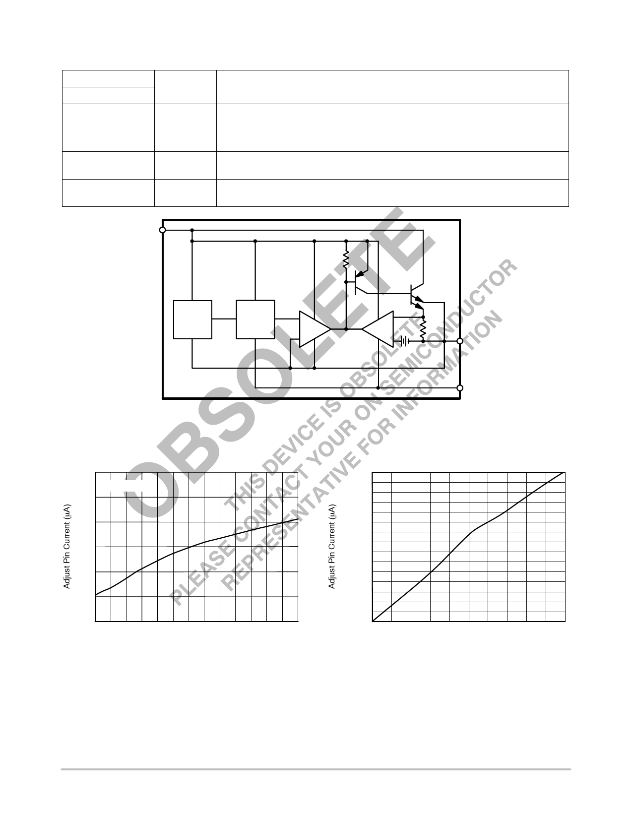
Figure 2. Block Diagram
TYPICAL PERFORMANCE CHARACTERISTICS
90
IO = 10 mA
85
80
75
70
65
60
0 10 20 30 40 50 60 70 80 90 100 110 120 130
TCASE (°C)
Figure 3. Adjust Pin Current Voltage vs.
Temperature
73.00
72.80
72.60
72.40
72.20
72.00
71.80
71.60
71.40
71.20
71.00
70.80
70.60
70.40
70.20
70.00
0
12345678
IOUT (A)
Figure 4. Adjust Pin vs. IOUT
9 10
http://onsemi.com
3
Share Link: 