SPT7937SIR 查看數據表(PDF) - Cadeka Microcircuits LLC.
零件编号
产品描述 (功能)
生产厂家
SPT7937SIR Datasheet PDF : 11 Pages
| |||
ABSOLUTE MAXIMUM RATINGS (Beyond which damage may occur)1 25 °C
Supply Voltages
AVDD ...................................................................... +6 V
DVDD ..................................................................... +6 V
OVDD ..................................................................... +6 V
Input Voltages
Analog Input ................................. –0.7 V to VDD +0.7 V
CLK Input ............................................................... VDD
AVDD – DVDD .................................................. ±100 mV
AGND – DGND .............................................. ±100 mV
Output
Digital Outputs .................................................... 10 mA
Temperature
Operating Temperature ........................... –40 to +85 °C
Junction Temperature ...................................... +175 °C
Lead Temperature, (soldering 10 seconds) ...... +300 °C
Storage Temperature ............................ –65 to +150 °C
Note 1: Operation at any Absolute Maximum Rating is not implied. See
Electrical Specifications for proper nominal applied conditions
in typical applications.
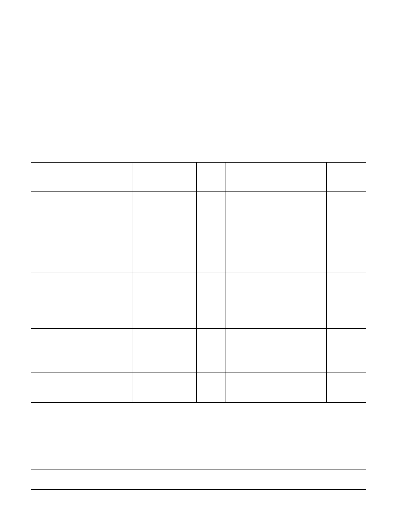
ELECTRICAL SPECIFICATIONS
TA=TMIN to TMAX, VDD=+5.0 V, ƒS=28 MSPS, VIN=0 to 4 V, VRHS=4.0 V, VRLS=0.0 V, unless otherwise specified.
PARAMETERS
TEST
CONDITIONS
TEST
LEVEL
MIN
SPT7937
TYP
Resolution
12
MAX
UNITS
Bits
DC Accuracy
Integral Linearity Error (ILE)
Differential Linearity Error (DLE)
No Missing Codes
V
±1.75
LSB
V
±0.9
LSB
VI
Guaranteed
Analog Input
Input Voltage Range
Input Capacitance
Input Bandwidth
Input Impedance
–Full-Scale Error1
+Full-Scale Error1
VI
VRLS
VRHS
V
V
5.0
pF
V
250
MHz
35
kΩ
V
1.0
LSB
V
0.12
%FS
Conversion Characteristics
Maximum Conversion Rate
Minimum Conversion Rate
Pipeline Delay (Latency)
Aperture Delay Time (TAP)
Aperture Jitter Time
Clock Duty Cycle
Over-Voltage Recovery Time2
VI
28
MHz
V
1
MHz
IV
14
Clock Cycles
V
1.0
ns
V
5.0
ps (RMS)
V
40
60
%
36
ns
Reference Input
Resistance
Voltage Range3
VRHS
VRLS
VRHS – VRLS
VI
350
500
650 Ω
IV
3.0
VDD
V
IV
0.0
2.0
V
V
1.0
4.0
5.0
V
Dynamic Performance
Effective Number of Bits
ƒIN = 3.58 MHz
ƒIN = 10 MHz
V
10.3
Bits
VI
10.0
Bits
1 The full-scale range spans the reference ladder sense pins, VRHS and VRLS. Refer to the Voltage Reference section for discussion.
2 Due to internal architecture, over-voltage recovery time is less than one clock cycle (i.e., 25 ns at ƒCLK = 40 MHz).
3 For optimum performance, the full-scale voltage range (VRHS–VRLS) should be between 3 V to 5 V.
SPT7937
2
3/5/02
Share Link: 