ZL30406 查看數據表(PDF) - Zarlink Semiconductor Inc
零件编号
产品描述 (功能)
生产厂家
ZL30406 Datasheet PDF : 21 Pages
| |||
ZL30406
Data Sheet
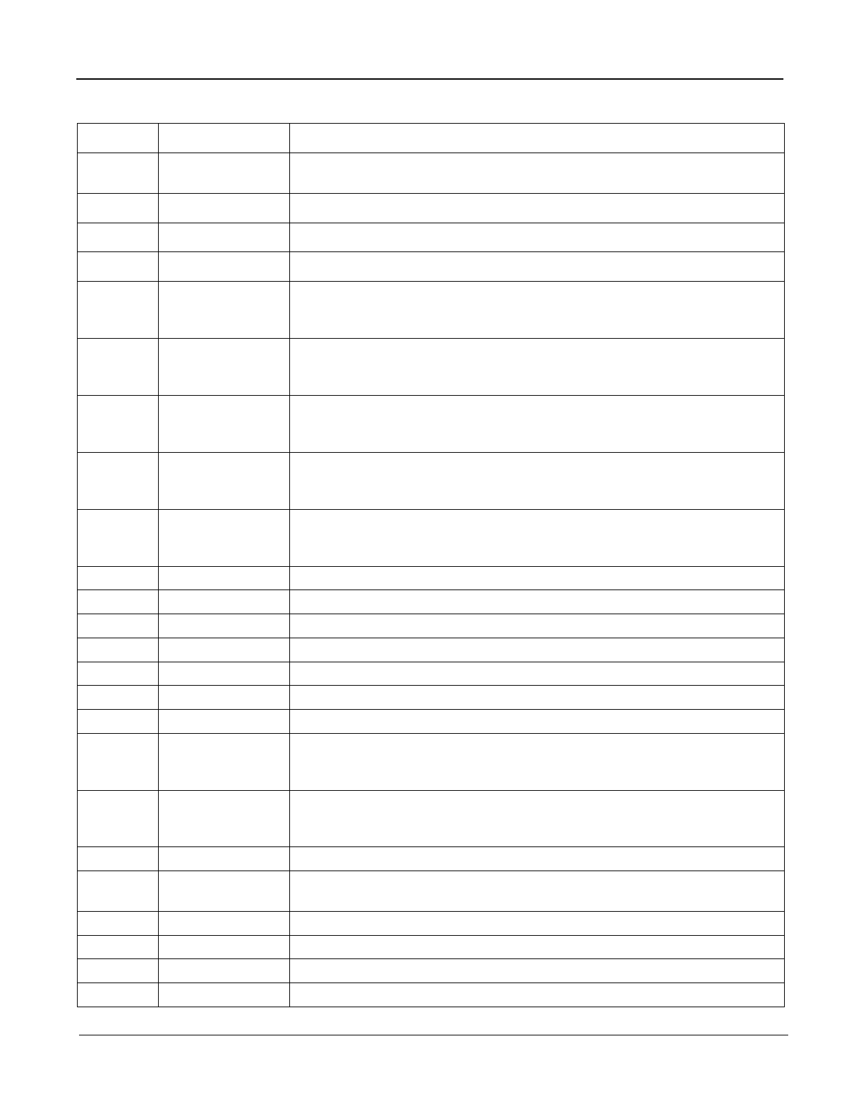
Pin Description Table (continued)
Pin #
8
9
10
11
12
13
14
15
16
17
18
19
20
21
22
23
24
25
26
27
28
29
30
31
32
Name
LPF
GND
GND
BIAS
OC-CLKoEN
C77oEN-A
C77oEN-B
C77oEN-C
C77oEN-D
GND
VDD
NC
NC
NC
VDD
IC
FS2
FS1
C19oEN
GND
C19i
VDD
GND
NC
GND
Description
Low Pass Filter (Analog). Connect to this pin external RC network (RF and CF)
for the low pass filter.
Ground. 0 volt
Ground. 0 volt
Bias. See Figure 11 for the recommended bias circuit.
SONET/SDH Clock Enable (CMOS Input). If tied high this control pin enables
the OC-CLKoP/N differential driver. Pulling this input low disables the output
clock without deactivating differential drivers.
C77 Clock Output Enable A (CMOS Input). If tied high this control pin
enables the C77oP/N-A output clock. Pulling this input low disables the output
clock without deactivating differential drivers.
C77 Clock Output Enable B (CMOS Input). If tied high this control pin
enables the C77oP/N-B output clock. Pulling this input low disables the output
clock without deactivating differential drivers.
C77 Clock Output Enable C (CMOS Input). If tied high this control pin
enables the C77oP/N-C output clock. Pulling this input low disables the output
clock without deactivating differential drivers.
C77 Clock Output Enable D (CMOS Input). If tied high this control pin
enables the C77oP/N-D output clock. Pulling this input low disables the output
clock without deactivating differential drivers.
Ground. 0 volt
Positive Digital Power Supply. +3.3 V ±10%
No internal bonding Connection. Leave unconnected.
No internal bonding Connection. Leave unconnected.
No internal bonding Connection. Leave unconnected.
Positive Digital Power Supply. +3.3 V ±10%
Internal Connection. Connect this pin to Ground (GND).
Frequency Select 2-1 (CMOS Input). These inputs program the clock
frequency on the OC-CLKo output. The possible output frequencies are
19.44 MHz (00), 38.88 MHz (01), 77.76 MHz (10), 155.52 MHz (11).
C19o Output Enable (CMOS Input). If tied high this control pin enables the
C19o output clock. Pulling this pin low forces output driver into a high
impedance state.
Ground. 0 volt
C19 Reference Input (CMOS Input). This pin is a single-ended input reference
source used for synchronization. This pin accepts 19.44 MHz.
Positive Digital Power Supply. +3.3 V ±10%
Ground. 0 volt
No internal bonding Connection. Leave unconnected.
Ground. 0 volt.
3
Zarlink Semiconductor Inc.
Share Link: 