ZL30406 查看數據表(PDF) - Zarlink Semiconductor Inc
零件编号
产品描述 (功能)
生产厂家
ZL30406 Datasheet PDF : 21 Pages
| |||
ZL30406
Data Sheet
1.4 Output Interface Circuit
The output of the VCO is used by the Output Interface Circuit to provide four LVPECL differential clocks at
77.76 MHz, one programmable CML differential clock (19.44 MHz, 38.88 MHz, 77.76 MHz, 155.52 MHz) controlled
with FS1-2 pins and a single-ended 19.44 MHz output clock. This block provides also a 19.44 MHz feedback clock
that closes PLL loop. Each output clock can be enabled or disabled individually with the associated Output Enable
pin.
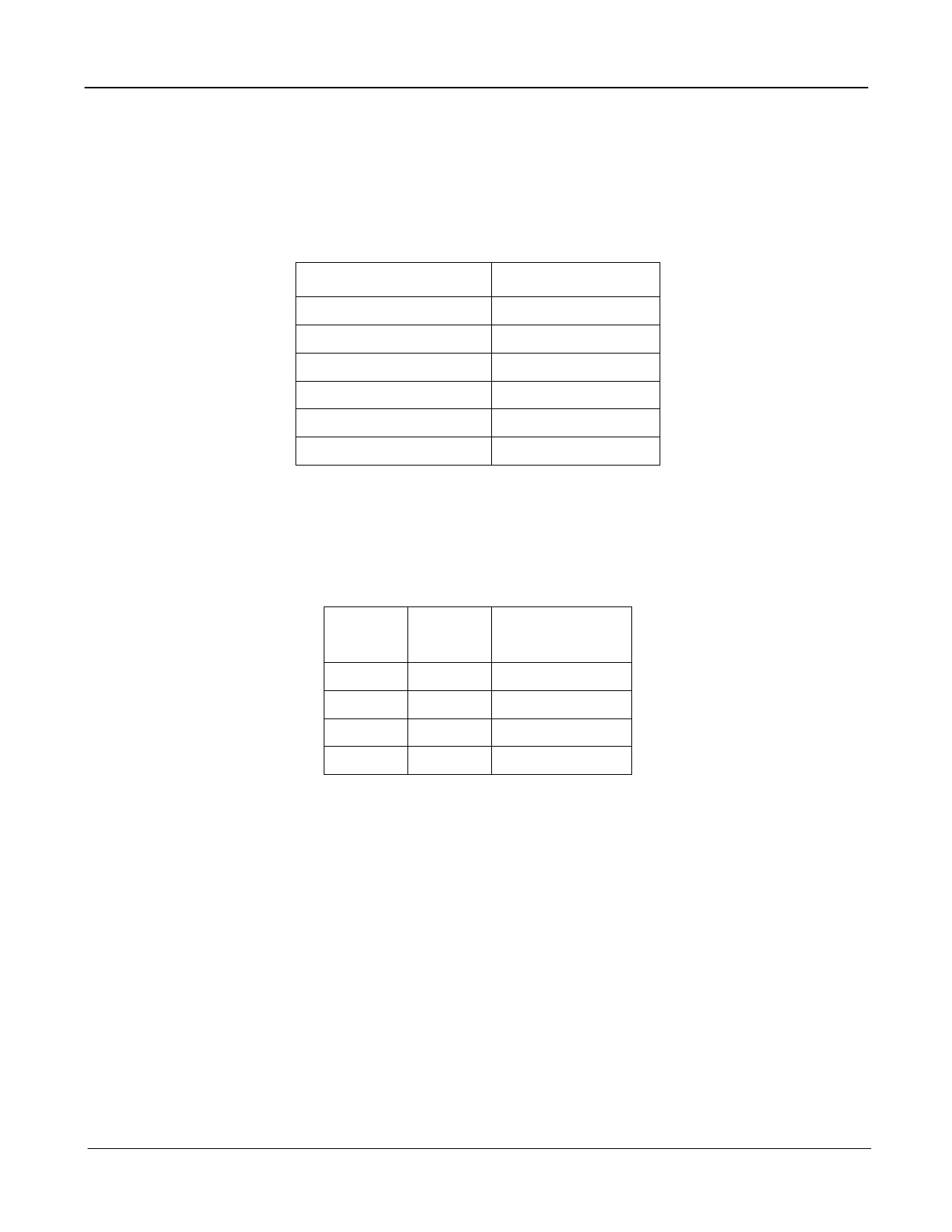
Output Clocks
Output Enable Pins
C77oP/N-A
C77oP/N-B
C77oP/N-C
C77oP/N-D
OC-CLKoP/N
C19o
C77oEN-A
C77oEN-B
C77oEN-C
C77oEN-D
OC-CLKoEN
C19oEN
Table 1 - Output Enable Control
To reduce power consumption and achieve the lowest possible intrinsic jitter the unused output clocks must be
disabled. If any of the LVPECL outputs are disabled they must be left open without any terminations.
The output clock frequency of the OC-CLKo CML differential output clock is selected with FS1-2 pins as shown in
the following table.
OC-CLKo
FS2
FS1
Frequency
0
0
19.44 MHz
0
1
38.88 MHz
1
0
77.76 MHz
1
1
155.52 MHz
Table 2 - OC-CLKo Clock Frequency Selection
6
Zarlink Semiconductor Inc.
Share Link: 