AD598 查看數據表(PDF) - Analog Devices
零件编号
产品描述 (功能)
生产厂家
AD598 Datasheet PDF : 16 Pages
| |||
AD598
8. C2, C3 and C4 are a function of the desired bandwidth of
the AD598 position measurement subsystem. They should
be nominally equal values.
C2 = C3 = C4 = 10–4 Farad Hz/fSUBSYSTEM (Hz)
If the desired system bandwidth is 250 Hz, then
C2 = C3 = C4 = 10–4 Farad Hz/250 Hz = 0.4 µF
See Figures 13, 14 and 15 for more information about
AD598 bandwidth and phase characterization.
9. In order to Compute R2, which sets the AD598 gain or full-
scale output range, several pieces of information are needed:
a. LVDT sensitivity, S
b. Full-scale core displacement, d
c. Ratio of manufacturer recommended primary drive level,
VPRI to (VA + VB) computed in Step 4.
LVDT sensitivity is listed in the LVDT manufacturer’s cata-
log and has units of millivolts output per volts input per inch
displacement. The E100 has a sensitivity of 2.4 mV/V/mil.
In the event that LVDT sensitivity is not given by the manu-
facturer, it can be computed. See section on Determining
LVDT Sensitivity.
For a full-scale displacement of d inches, voltage out of the
AD598 is computed as
VOUT
=
S
×
VPRI
(VA +VB )
× 500
µA ×
R2 ×
d.
VOUT is measured with respect to the signal reference,
Pin 17 shown in Figure 7.
Solving for R2,
R2 =
VOUT × (VA +VB )
S ×VPRI × 500 µA × d
(1)
Note that VPRI is the same signal level used in Step 4 to
determine (VA + VB).
For VOUT = 20 V full-scale range (± 10 V) and d = 0.2 inch
full-scale displacement (± 0.1 inch),
R2
=
2. 4
20 V
× 3×
× 2.70V
500 µA ×
0. 2
=
75. 3 kΩ
VOUT as a function of displacement for the above example is
shown in Figure 9.
VOUT (VOLTS)
+10
–0.1
+0.1 d (INCHES)
–10
Figure 9. VOUT (±10 V Full Scale)
vs. Core Displacement (±0.1 Inch)
10. Selections of R3 and R4 permit a positive or negative output
voltage offset adjustment.
VOS
= 1.2V
×
R2
×
R
3
+
1
5
kΩ*
–
R4
1
+ 5 kΩ*
(2)
*These values have a ± 20% tolerance.
For no offset adjustment R3 and R4 should be open circuit.
To design a circuit producing a 0 V to +10 V output for a
displacement of ± 0.1 inch, set VOUT to +10 V, d = 0.2 inch
and solve Equation (1) for R2.
R2 = 37.6 kΩ
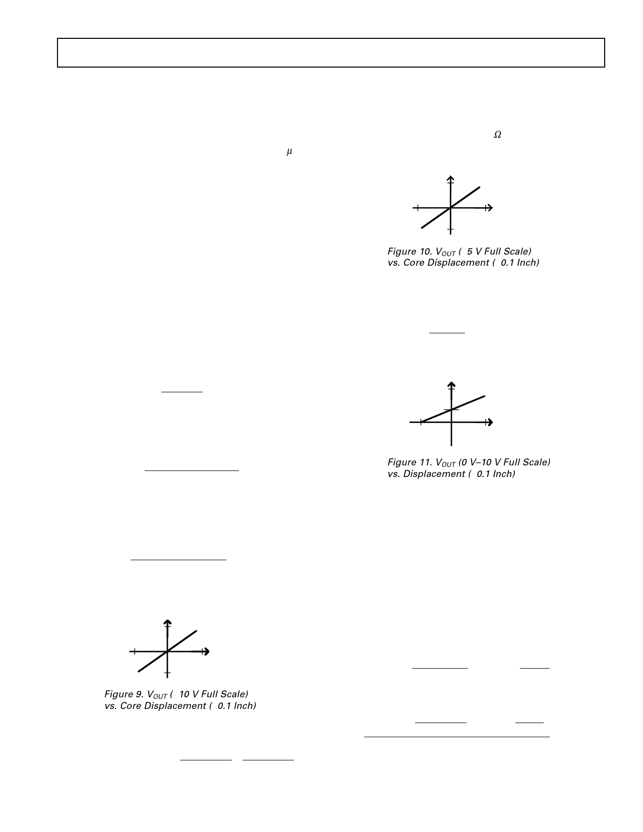
This will produce a response shown in Figure 10.
VOUT (VOLTS)
+5
–0.1
+0.1 d (INCHES)
–5
Figure 10. VOUT (±5 V Full Scale)
vs. Core Displacement (±0.1 Inch)
In Equation (2) set VOS = 5 V and solve for R3 and R4.
Since a positive offset is desired, let R4 be open circuit.
Rearranging Equation (2) and solving for R3
R
3
=
1.2 × R2
VOS
–
5
kΩ
=
4. 02
kΩ
Figure 11 shows the desired response.
VOUT (VOLTS)
+10
+5
–0.1
+0.1 d (INCHES)
Figure 11. VOUT (0 V–10 V Full Scale)
vs. Displacement (±0.1 Inch)
DESIGN PROCEDURE
SINGLE SUPPLY OPERATION
Figure 12 shows the single supply connection method.
For single supply operation, repeat Steps 1 through 10 of the
design procedure for dual supply operation, then complete the
additional Steps 11 through 14 below. R5, R6 and C5 are addi-
tional component values to be determined. VOUT is measured
with respect to SIGNAL REFERENCE.
11. Compute a maximum value of R5 and R6 based upon the
relationship
R5 + R6 ≤ VPS/100 µA
12. The voltage drop across R5 must be greater than
2
+
10
kΩ
*
R4
1. 2V
+ 5 kΩ
Therefore
+
250
µA
+
VOUT
4 × R2
Volts
R5≥
2 +10
kΩ*
1.2 V
R4 +5kΩ
100
+ 250
µA
µA
+
V OUT
4 × R2
Ohms
*These values have ± 20% tolerance.
Based upon the constraints of R5 + R6 (Step 11) and R5
(Step 12), select an interim value of R6.
REV. A
–7–
Share Link: 