HIP4086 查看數據表(PDF) - Renesas Electronics
零件编号
产品描述 (功能)
生产厂家
HIP4086 Datasheet PDF : 17 Pages
| |||
HIP4086, HIP4086A
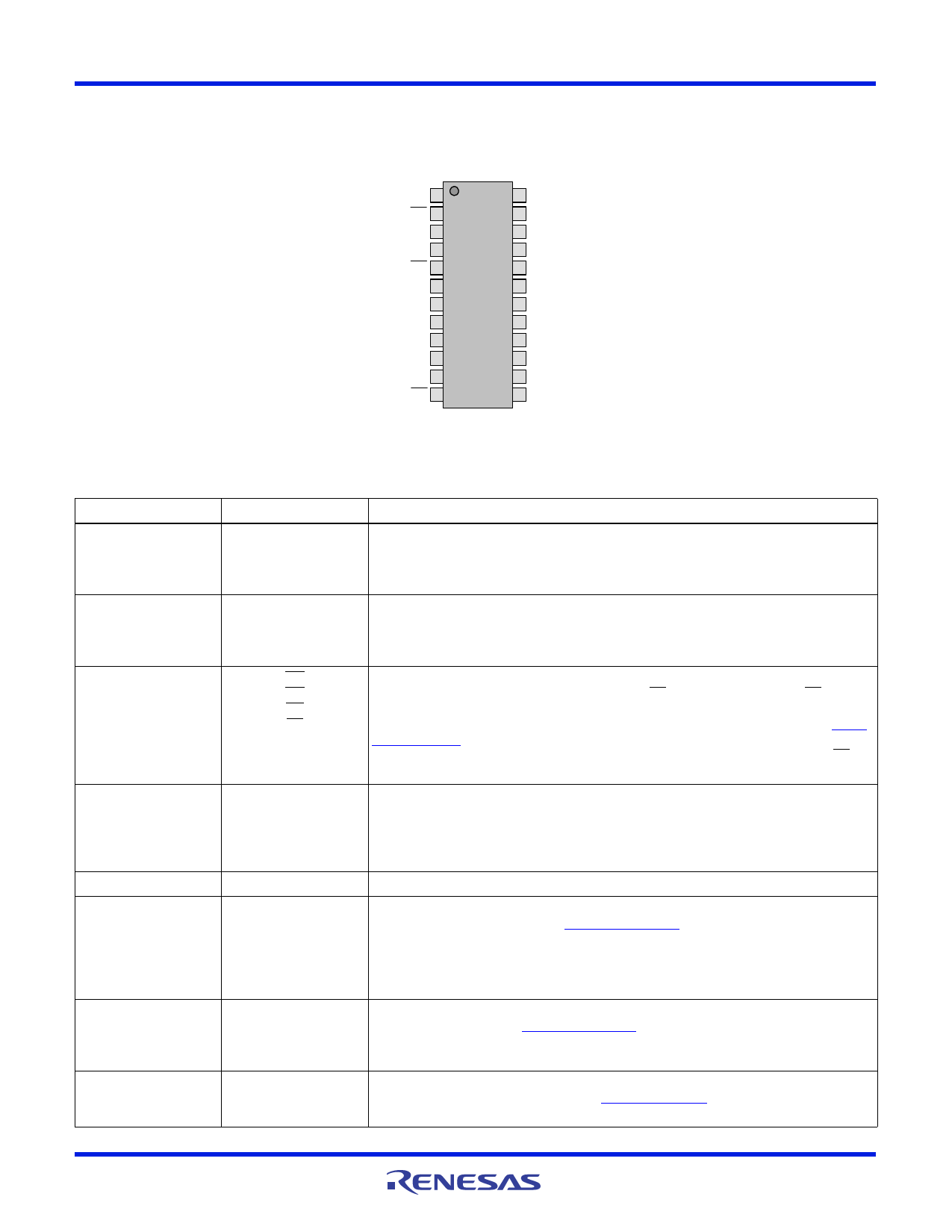
Pin Configuration
HIP4086, HIP4086A
(24 LD PDIP, SOIC)
TOP VIEW
BHB 1
BHI 2
BLI 3
ALI 4
AHI 5
VSS 6
RDEL 7
UVLO 8
RFSH 9
DIS 10
CLI 11
CHI 12
24 BHO
23 BHS
22 BLO
21 ALO
20 VDD
19 CLO
18 AHS
17 AHO
16 AHB
15 CHS
14 CHO
13 CHB
Pin Descriptions
PIN NUMBER
16
1
13
18
23
15
5
2
12
SYMBOL
AHB
BHB
CHB
(xHB)
AHS
BHS
CHS
(xHS)
AHI
BHI
CHI
(xHI)
4
ALI
3
BLI
11
CLI
(xLI)
6
VSS
7
RDEL
8
9
FN4220 Rev 1.00
January 12, 2017
UVLO
RFSH
DESCRIPTION
High-Side Bias Connections. One external bootstrap diode and one capacitor are required for
each. Connect cathode of bootstrap diode and positive side of bootstrap capacitor to each xHB
pin.
High-Side Source Connections. Connect the sources of the high-side power MOSFETs to these
pins. The negative side of the bootstrap capacitors are also connected to these pins.
High-Side Logic Level Inputs. Logic at these three pins controls the three high-side output drivers,
AHO (Pin 17), BHO (Pin 24) and CHO (Pin 14). When xHI is low, xHO is high. When xHI is high,
xHO is low. Unless the dead time is disabled by connecting RDEL (Pin 7) to ground, the low-side
input of each phase will override the corresponding high-side input on that phase - see “Truth
Table” on page 2. If RDEL is tied to ground, dead time is disabled and the outputs follow the
inputs with no shoot-through protection. DIS (Pin 10) also overrides the high-side inputs. xHI can
be driven by signal levels of 0V to 15V (no greater than VDD).
Low-Side Logic Level Inputs. Logic at these three pins controls the three low-side output drivers
ALO (Pin 21), BLO (Pin 22) and CLO (Pin 19). If the upper inputs are grounded then the lower
inputs control both xLO and xHO drivers, with the dead time set by the resistor at RDEL (Pin 7).
DIS (Pin 10) high level input overrides xLI, forcing all outputs low. xLI can be driven by signal
levels of 0V to 15V (no greater than VDD).
Ground. Connect the sources of the low-side power MOSFETs to this pin.
Delay Time Set Point. Connect a resistor from this pin to VDD to set timing current that defines
the dead time between drivers - see Figure 19 on page 10. All drivers turn off with minimal
delay, RDEL resistor prevents shoot-through by delaying the turn-on of all drivers. When RDEL is
tied to VSS, both upper and lowers can be commanded on simultaneously. While not necessary
in most applications, a decoupling capacitor of 0.1µF or smaller may be connected between
RDEL and VSS.
Undervoltage Set Point. A resistor can be connected between this pin and VSS to program the
undervoltage set point - see Figure 20 on page 10. With this pin not connected, the under
voltage disable is typically 6.6V. When this pin is tied to VDD, the under voltage disable is
typically 6.2V.
Refresh Pulse Setting. An external capacitor can be connected from this pin to VSS to increase
the length of the start up refresh pulse - see Figure 18 on page 9. If this pin is not connected, the
refresh pulse is typically 1.5µs.
Page 3 of 17
Share Link: 