WM8199 查看數據表(PDF) - Cirrus Logic
零件编号
产品描述 (功能)
生产厂家
WM8199 Datasheet PDF : 32 Pages
| |||
WM8199
Production Data
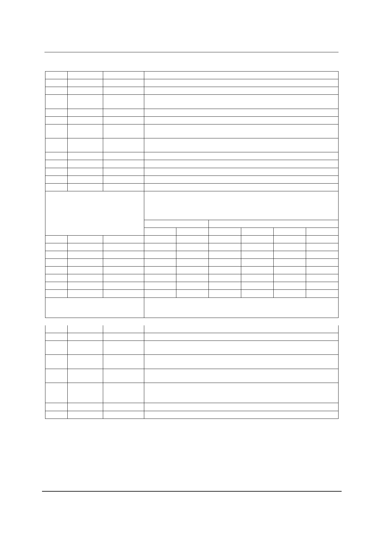
PIN DESCRIPTION
PIN
NAME
TYPE
DESCRIPTION
1
RINP
Analogue input Red channel input video.
2
AGND2
Supply
Analogue ground (0V).
3
DVDD1
Supply
Digital supply (5V) for logic and clock generator. This must be operated at the same
potential as AVDD.
4
OEB
Digital input Output Hi-Z control, all digital outputs disabled when OEB = 1.
5
VSMP
Digital input Video sample synchronisation pulse.
6
RLC/ACYC Digital input RLC (active high) selects reset level clamp on a pixel-by-pixel basis – tie high if
used on every pixel. ACYC autocycles between R, G, B inputs.
7
MCLK
Digital input Master clock. This clock is applied at N times the input pixel rate (N = 2, 3, 6, 8 or
any multiple of 2 thereafter depending on input sample mode).
8
DGND
Supply
Digital ground (0V).
9
SEN
Digital input Enables the serial interface when high.
10
DVDD2
Supply
Digital supply (5V/3.3V), all digital I/O pins.
11
SDI
Digital input Serial data input.
12
SCK
Digital input Serial clock.
Digital multiplexed output data bus.
ADC output data (d15:d0) is available in two multiplexed formats as shown, under
the control of register MUXOP [1:0]
See ‘Output Formats’ description in Device Description section for further details.
8+8-bit
4+4+4+4-bit
A
B
A
B
C
D
13
OP[0]
Digital output
d8
d0
14
OP[1]
Digital output
d9
d1
15
OP[2]
Digital output
d10
d2
16
OP[3]
Digital output
d11
d3
17
OP[4]
Digital output
d12
d4
d12
d8
d4
d0
18
OP[5]
Digital output
d13
d5
d13
d9
d5
d1
19
OP[6]
Digital output
d14
d6
d14
d10
d6
d2
20
OP[7]/SDO Digital output
d15
d7
d15
d11
d7
d3
Alternatively, pin OP[7]/SDO may be used to output register read-back data when
OEB = 0 and SEN has been pulsed high. See Serial Interface description in Device
Description section for further details.
21
AVDD
Supply
Analogue supply (5V). This must be operated at the same potential as DVDD1.
22
AGND1
Supply
Analogue ground (0V).
23
VRB
Analogue output Lower reference voltage.
This pin must be connected to AGND via a decoupling capacitor.
24
VRT
Analogue output Upper reference voltage.
This pin must be connected to AGND via a decoupling capacitor.
25
VRX
Analogue output Input return bias voltage.
This pin must be connected to AGND via a decoupling capacitor.
26 VRLC/VBIAS Analogue I/O Selectable analogue output voltage for RLC or single-ended bias reference.
This pin would typically be connected to AGND via a decoupling capacitor.
VRLC can be externally driven if programmed Hi-Z.
27
BINP
Analogue input Blue channel input video.
28
GINP
Analogue input Green channel input video.
w
PD, Rev 4.4, July 2008
4
Share Link: 